JAJS397F August 2009 – July 2016 TPA3111D1
PRODUCTION DATA.
- 1 特長
- 2 アプリケーション
- 3 概要
- 4 改訂履歴
- 5 Pin Configuration and Functions
- 6 Specifications
- 7 Detailed Description
-
8 Application and Implementation
- 8.1 Application Information
- 8.2
Typical Application
- 8.2.1 Design Requirements
- 8.2.2
Detailed Design Procedure
- 8.2.2.1 Ferrite Bead Filter Considerations
- 8.2.2.2 Efficiency: LC Filter Required With the Traditional Class-D Modulation Scheme
- 8.2.2.3 When to Use an Output Filter for EMI Suppression
- 8.2.2.4 Input Resistance
- 8.2.2.5 Input Capacitor, CI
- 8.2.2.6 BSN and BSP Capacitors
- 8.2.2.7 Differential Inputs
- 8.2.2.8 Using Low-ESR Capacitors
- 8.2.3 Application Curves
- 9 Power Supply Recommendations
- 10Layout
- 11デバイスおよびドキュメントのサポート
- 12メカニカル、パッケージ、および注文情報
パッケージ・オプション
メカニカル・データ(パッケージ|ピン)
- PWP|28
サーマルパッド・メカニカル・データ
- PWP|28
発注情報
6 Specifications
6.1 Absolute Maximum Ratings
over operating free-air temperature range (unless otherwise noted)(1)| MIN | MAX | UNIT | ||
|---|---|---|---|---|
| Supply voltage, VCC | AVCC, PVCC | –0.3 | 30 | V |
| Interface pin voltage, VI | SD, FAULT, GAIN0, GAIN1, AVCC (Pin 14)(2) | –0.3 | VCC + 0.3 | V |
| <10 | V/ms | |||
| PLIMIT | –0.3 | VGVDD + 0.3 | V | |
| INN, INP | –0.3 | 6.3 | ||
| Minimum load resistance, RL | BTL | 3.2 | Ω | |
| Continuous total power dissipation | See Thermal Information | |||
| Operating free-air temperature, TA | –40 | 85 | °C | |
| Operating junction temperature, TJ(3) | –40 | 150 | °C | |
| Storage temperature, Tstg | –65 | 150 | °C | |
(1) Stresses beyond those listed under Absolute Maximum Ratings may cause permanent damage to the device. These are stress ratings only, which do not imply functional operation of the device at these or any other conditions beyond those indicated under Recommended Operating Conditions. Exposure to absolute-maximum-rated conditions for extended periods may affect device reliability.
(2) The voltage slew rate of these pins must be restricted to no more than 10 V/ms. For higher slew rates, use a 100-kΩ resistor in series with the pins.
(3) The TPA3111D1 incorporates an exposed thermal pad on the underside of the chip. This acts as a heatsink, and it must be connected to a thermally dissipating plane for proper power dissipation. Failure to do so may result in the device going into thermal protection shutdown. See Quad Flatpack No-Lead Logic Packages and QFN/SON PCB Attachment for more information about using the QFN thermal pad. See PowerPad™ Thermally Enhanced package for more information about using the HTQFP thermal pad.
6.2 ESD Ratings
| VALUE | UNIT | |||
|---|---|---|---|---|
| V(ESD) | Electrostatic discharge | Human-body model (HBM)(1) | ±2000 | V |
| Charged-device model (CDM)(2) | ±500 | |||
(1) In accordance with JEDEC Standard 22, Test Method A114-B.
(2) In accordance with JEDEC Standard 22, Test Method C101-A
6.3 Recommended Operating Conditions
over operating free-air temperature range (unless otherwise noted)| MIN | MAX | UNIT | |||
|---|---|---|---|---|---|
| VCC | Supply voltage | PVCC, AVCC | 8 | 26 | V |
| VIH | High-level input voltage | SD, GAIN0, GAIN1 | 2 | V | |
| VIL | Low-level input voltage | SD, GAIN0, GAIN1 | 0.8 | V | |
| VOL | Low-level output voltage | FAULT, RPULLUP = 100 kΩ, VCC = 26 V | 0.8 | V | |
| IIH | High-level input current | SD, GAIN0, GAIN1, VI = 2 V, VCC = 18 V | 50 | µA | |
| IIL | Low-level input current | SD, GAIN0, GAIN1, VI = 0.8 V, VCC = 18 V | 5 | µA | |
6.4 Thermal Information
| THERMAL METRIC(1)(2) | TPA3111D1 | UNIT | |
|---|---|---|---|
| PWP (HTSSOP) | |||
| 28 PINS | |||
| RθJA | Junction-to-ambient thermal resistance | 30.3 | °C/W |
| RθJC(top) | Junction-to-case (top) thermal resistance | 33.5 | °C/W |
| RθJB | Junction-to-board thermal resistance | 17.5 | °C/W |
| ψJT | Junction-to-top characterization parameter | 0.9 | °C/W |
| ψJB | Junction-to-board characterization parameter | 7.2 | °C/W |
| RθJC(bot) | Junction-to-case (bottom) thermal resistance | 0.9 | °C/W |
(1) For more information about traditional and new thermal metrics, see the Semiconductor and IC Package Thermal Metrics application report.
(2) For thermal estimates of this device based on PCB copper area, see the TI PCB Thermal Calculator.
6.5 DC Characteristics – VCC = 24 V
TA = 25°C, RL = 8 Ω (unless otherwise noted)| PARAMETER | TEST CONDITIONS | MIN | TYP | MAX | UNIT | ||
|---|---|---|---|---|---|---|---|
| |VOS| | Class-D output offset voltage (measured differentially) | VI = 0 V, Gain = 36 dB | 1.5 | 15 | mA | ||
| ICC | Quiescent supply current | SD = 2 V, no load, PVCC = 21 V | 40 | mA | |||
| ICC(SD) | Quiescent supply current in shutdown mode | SD = 0.8 V, no load, PVCC = 21 V | 400 | µA | |||
| RDS(ON) | Drain-source ON-state resistance | IO = 500 mA, TJ = 25°C | High side | 240 | mΩ | ||
| Low side | 240 | ||||||
| G | Gain | VGAIN1 = 0.8 V | VGAIN0 = 0.8 V | 19 | 20 | 21 | dB |
| VGAIN0 = 2 V | 25 | 26 | 27 | ||||
| VGAIN1 = 2 V | VGAIN0 = 0.8 V | 31 | 32 | 33 | |||
| VGAIN0 = 2 V | 35 | 36 | 37 | ||||
| tON | Turnon time | VSD = 2 V | 10 | ms | |||
| tOFF | Turnoff time | VSD = 0.8 V | 2 | µs | |||
| VGVDD | Gate drive supply | IGVDD = 2 mA | 6.5 | 6.9 | 7.3 | V | |
6.6 DC Characteristics – VCC = 12 V
TA = 25°C, RL = 8 Ω (unless otherwise noted)| PARAMETER | TEST CONDITIONS | MIN | TYP | MAX | UNIT | ||
|---|---|---|---|---|---|---|---|
| |VOS| | Class-D output offset voltage (measured differentially) | VI = 0 V, Gain = 36 dB | 1.5 | 15 | mA | ||
| ICC | Quiescent supply current | SD = 2 V, no load, PVCC = 12 V | 20 | mA | |||
| ICC(SD) | Quiescent supply current in shutdown mode | SD = 0.8 V, no load, PVCC = 12 V | 200 | µA | |||
| RDS(ON) | Drain-source ON-state resistance | IO = 500 mA, TJ = 25°C | High side | 240 | mΩ | ||
| Low side | 240 | ||||||
| G | Gain | VGAIN1 = 0.8 V | VGAIN0 = 0.8 V | 19 | 20 | 21 | dB |
| VGAIN0 = 2 V | 25 | 26 | 27 | ||||
| VGAIN1 = 2 V | VGAIN0 = 0.8 V | 31 | 32 | 33 | |||
| VGAIN0 = 2 V | 35 | 36 | 37 | ||||
| tON | Turnon time | VSD = 2 V | 10 | ms | |||
| tOFF | Turnoff time | VSD = 0.8 V | 2 | µs | |||
| VGVDD | Gate drive supply | IGVDD = 2 mA | 6.5 | 6.9 | 7.3 | V | |
| PLIMIT | Output voltage maximum under PLIMIT control | VPLIMIT = 2 V, VI = 6 V differential | 6.75 | 7.9 | 8.75 | V | |
6.7 AC Characteristics – VCC = 24 V
TA = 25°C, RL = 8 Ω (unless otherwise noted)| PARAMETER | TEST CONDITIONS | MIN | TYP | MAX | UNIT | |
|---|---|---|---|---|---|---|
| KSVR | Power supply ripple rejection | 200-mVPP ripple from 20 Hz to 1 kHz, Gain = 20 dB, Inputs AC-coupled to AGND |
–70 | dB | ||
| PO | Continuous output power | f = 1 kHz, VCC = 24 V, THD+N ≤ 0.1% | 10 | W | ||
| THD+N | Total harmonic distortion + noise | f = 1 kHz, VCC = 24 V, PO = 5 W (half-power) | <0.05% | |||
| VN | Output integrated noise | 20 Hz to 22 kHz, A-weighted filter, Gain = 20 dB | 65 | µV | ||
| –80 | dBV | |||||
| Crosstalk | f = 1 kHz, VO = 1 Vrms, Gain = 20 dB | –70 | dB | |||
| SNR | Signal-to-noise ratio | Maximum output at THD+N < 1%, f = 1 kHz, Gain = 20 dB, A-weighted |
102 | dB | ||
| fOSC | Oscillator frequency | 250 | 310 | 350 | kHz | |
| Thermal trip point | 150 | °C | ||||
| Thermal hysteresis | 15 | °C | ||||
6.8 AC Characteristics – VCC = 12 V
TA = 25°C, RL = 8 Ω (unless otherwise noted)| PARAMETER | TEST CONDITIONS | MIN | TYP | MAX | UNIT | |
|---|---|---|---|---|---|---|
| KSVR | Power supply ripple rejection | 200-mVPP ripple from 20 Hz to 1 kHz, Gain = 20 dB, Inputs AC-coupled to AGND |
–70 | dB | ||
| PO | Continuous output power | f = 1 kHz, RL = 8 Ω, THD+N ≤ 10% | 10 | W | ||
| f = 1 kHz, RL = 4 Ω, THD+N ≤ 0.1% | 10 | |||||
| THD+N | Total harmonic distortion + noise | f = 1 kHz, RL = 8 Ω, PO = 5 W (half-power) | <0.06% | |||
| VN | Output integrated noise | 20 Hz to 22 kHz, A-weighted filter, Gain = 20 dB | 65 | µV | ||
| –80 | dBV | |||||
| Crosstalk | f = 1 kHz, PO = 1 W, Gain = 20 dB | –70 | dB | |||
| SNR | Signal-to-noise ratio | Maximum output at THD+N < 1%, f = 1 kHz, Gain = 20 dB, A-weighted |
102 | dB | ||
| fOSC | Oscillator frequency | 250 | 310 | 350 | kHz | |
| Thermal trip point | 150 | °C | ||||
| Thermal hysteresis | 15 | °C | ||||
6.9 Typical Characteristics
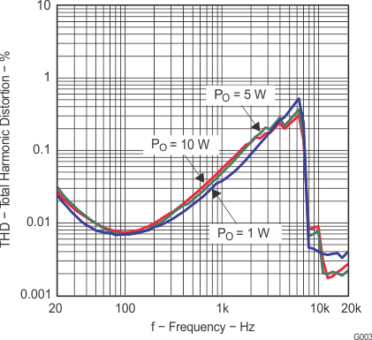
All measurements taken at 1 kHz, unless otherwise noted. Measurements were made using the TPA3111D1 EVM.
| Gain = 20 dB | VCC = 12 V | ZL = 8 Ω + 66 µH |
| Gain = 20 dB | VCC = 12 V | ZL = 4 Ω + 33 µH |
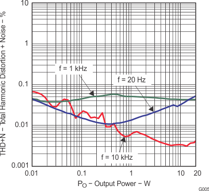
| Gain = 20 dB | VCC = 24 V | ZL = 8 Ω + 66 µH |
vs Output Power
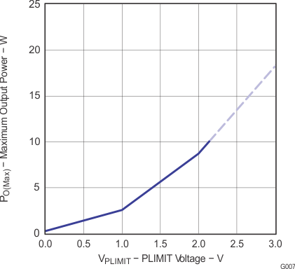
Dashed line represents thermally limited region.
Figure 7. Maximum Output Power vs PLIMIT Voltage
| Gain = 20 dB | VCC = 24 V | ZL = 8 Ω + 66 µH |
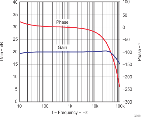
| Gain = 20 dB | VCC = 12 V | ZL = 8 Ω + 66 µH |
| CI = µF | VI = 0.1 VRMS | |
| Filter = Audio Precision AUX-0225 | ||
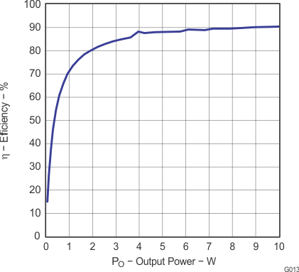
| Gain = 20 dB | VCC = 12 V | ZL = 4 Ω + 33 µH |
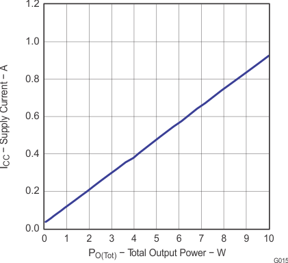
| Gain = 20 dB | VCC = 12 V | ZL = 4 Ω + 33 µH |
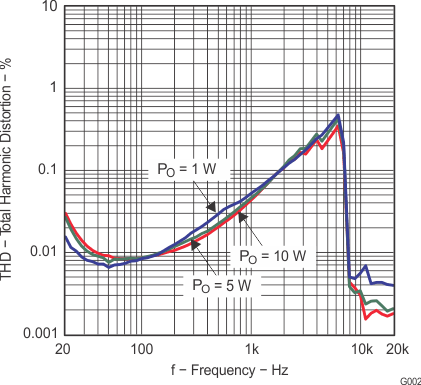
| Gain = 20 dB | VCC = 24 V | ZL = 8 Ω + 66 µH |
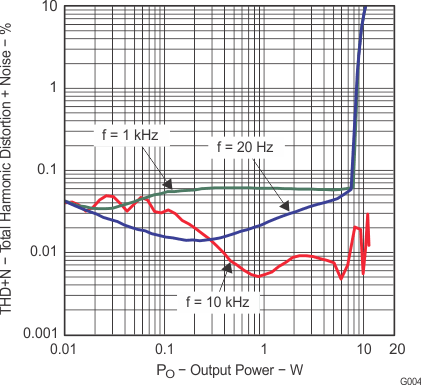
| Gain = 20 dB | VCC = 12 V | ZL = 8 Ω + 66 µH |
vs Output Power
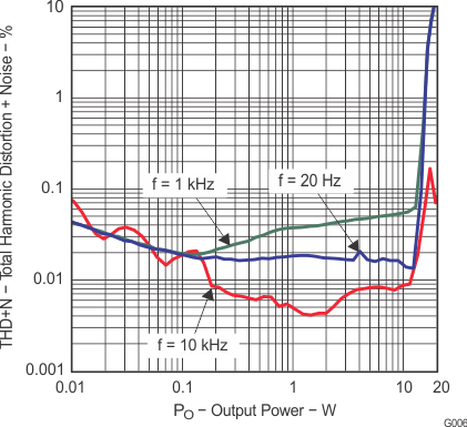
| Gain = 20 dB | VCC = 12 V | ZL = 4 Ω + 33 µH |
vs Output Power

Dashed line represents thermally limited region.
Figure 8. Output Power vs PLIMIT Voltage
| Gain = 20 dB | VCC = 12 V | ZL = 4 Ω + 33 µH |
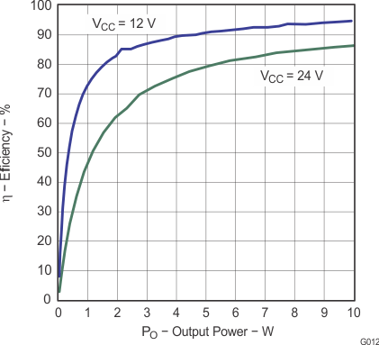
| Gain = 20 dB | ZL = 8 Ω + 66 µH | |
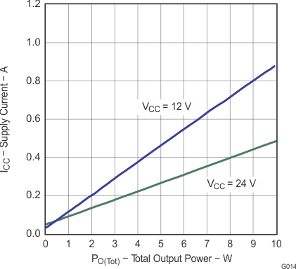
| Gain = 20 dB | ZL = 8 Ω + 66 µH |
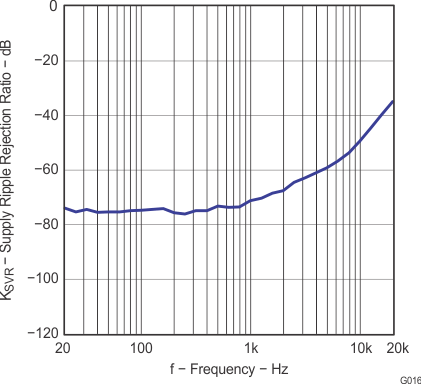
| Gain = 20 dB | VCC = 12 V | ZL = 8 Ω + 66 µH |