JAJSF52 April 2018 TPA3126D2
PRODUCTION DATA.
- 1 特長
- 2 アプリケーション
- 3 概要
- 4 改訂履歴
- 5 Device Comparison Table
- 6 Pin Configuration and Functions
- 7 Specifications
-
8 Detailed Description
- 8.1 Overview
- 8.2 Functional Block Diagram
- 8.3
Feature Description
- 8.3.1 Gain Setting and Master and Slave
- 8.3.2 Input Impedance
- 8.3.3 Startup and Shutdown Operation
- 8.3.4 PLIMIT Operation
- 8.3.5 GVDD Supply
- 8.3.6 BSPx and BSNx Capacitors
- 8.3.7 Differential Inputs
- 8.3.8 Device Protection System
- 8.3.9 DC Detect Protection
- 8.3.10 Short-Circuit Protection and Automatic Recovery Feature
- 8.3.11 Thermal Protection
- 8.3.12 Device Modulation Scheme
- 8.3.13 Efficiency: LC Filter Required with the Traditional Class-D Modulation Scheme
- 8.3.14 Ferrite Bead Filter Considerations
- 8.3.15 When to Use an Output Filter for EMI Suppression
- 8.3.16 AM Avoidance EMI Reduction
- 8.4 Device Functional Modes
- 9 Application and Implementation
- 10Power Supply Recommendations
- 11Layout
- 12デバイスおよびドキュメントのサポート
- 13メカニカル、パッケージ、および注文情報
パッケージ・オプション
メカニカル・データ(パッケージ|ピン)
- DAD|32
サーマルパッド・メカニカル・データ
- DAD|32
発注情報
8.3.12.1 BD Modulation
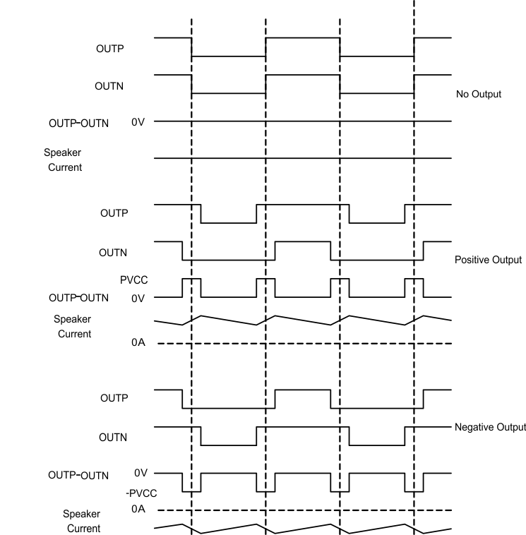
This is a modulation scheme that allows operation without the classic LC reconstruction filter when the amplifier is driving an inductive load with short speaker wires. Each output is switching from 0 volts to the supply voltage. The OUTPx and OUTNx are in phase with each other with no input so that there is little or no current in the speaker. The duty cycle of OUTPx is greater than 50% and OUTNx is less than 50% for positive output voltages. The duty cycle of OUTPx is less than 50% and OUTNx is greater than 50% for negative output voltages. The voltage across the load sits at 0V throughout most of the switching period, reducing the switching current, which reduces any I2R losses in the load.
 Figure 28. BD Mode Modulation