JAJSCV9C May 2016 – January 2018 TPA3128D2 , TPA3129D2
PRODUCTION DATA.
- 1 特長
- 2 アプリケーション
- 3 概要
- 4 改訂履歴
- 5 Pin Configuration and Functions
- 6 Specifications
-
7 Detailed Description
- 7.1 Overview
- 7.2 Functional Block Diagram
- 7.3
Feature Description
- 7.3.1 Gain Setting and Master and Slave
- 7.3.2 Input Impedance
- 7.3.3 Startup and Shutdown Operation
- 7.3.4 PLIMIT Operation
- 7.3.5 GVDD Supply
- 7.3.6 BSPx AND BSNx Capacitors
- 7.3.7 Differential Inputs
- 7.3.8 Device Protection System
- 7.3.9 DC Detect Protection
- 7.3.10 Short-Circuit Protection and Automatic Recovery Feature
- 7.3.11 Thermal Protection
- 7.3.12 Device Modulation Scheme
- 7.3.13 Efficiency: LC Filter Required with the Traditional Class-D Modulation Scheme
- 7.3.14 Ferrite Bead Filter Considerations
- 7.3.15 When to Use an Output Filter for EMI Suppression
- 7.3.16 AM Avoidance EMI Reduction
- 7.4 Device Functional Modes
- 8 Applications and Implementation
- 9 Power Supply Recommendations
- 10Layout
- 11デバイスおよびドキュメントのサポート
- 12メカニカル、パッケージ、および注文情報
パッケージ・オプション
メカニカル・データ(パッケージ|ピン)
- DAP|32
サーマルパッド・メカニカル・データ
- DAP|32
発注情報
7.3.14 Ferrite Bead Filter Considerations
Using the Advanced Emissions Suppression Technology in the TPA3128D2 and TPA3129D2 amplifiers, a high efficiency class-D audio amplifier can be designed while minimizing interference to surrounding circuits. Designing the amplifier can also be accomplished with only a low-cost ferrite bead filter. In this case the user must carefully select the ferrite bead used in the filter. One important aspect of the ferrite bead selection is the type of material used in the ferrite bead. Not all ferrite material is alike, therefore the user must select a material that is effective in the 10-MHz to 100-MHz range which is key to the operation of the class-D amplifier. Many of the specifications regulating consumer electronics have emissions limits as low as 30 MHz. The ferrite bead filter should be used to block radiation in the 30-MHz and above range from appearing on the speaker wires and the power supply lines which are good antennas for these signals. The impedance of the ferrite bead can be used along with a small capacitor with a value in the range of 1000 pF to reduce the frequency spectrum of the signal to an acceptable level. For best performance, the resonant frequency of the ferrite bead/ capacitor filter should be less than 10 MHz.
Also, the ferrite bead must be large enough to maintain its impedance at the peak currents expected for the amplifier. Some ferrite bead manufacturers specify the bead impedance at a variety of current levels. In this case the user can make sure the ferrite bead maintains an adequate amount of impedance at the peak current the amplifier will see. If these specifications are not available, the device can also estimate the bead current handling capability by measuring the resonant frequency of the filter output at low power and at maximum power. A change of resonant frequency of less than fifty percent under this condition is desirable. Examples of ferrite beads which have been tested and work well with the TPA3136D2 can be seen in the TPA3136D2EVM user guide SLOU444.
A high quality ceramic capacitor is also required for the ferrite bead filter. A low ESR capacitor with good temperature and voltage characteristics will work best.
Additional EMC improvements may be obtained by adding snubber networks from each of the class-D outputs to ground. Suggested values for a simple RC series snubber network would be 18 Ω in series with a 330 pF capacitor although design of the snubber network is specific to every application and must be designed taking into account the parasitic reactance of the printed circuit board as well as the audio amp. Take care to evaluate the stress on the component in the snubber network especially if the amp is running at high PVCC. Also, make sure the layout of the snubber network is tight and returns directly to the GND pins on the IC.
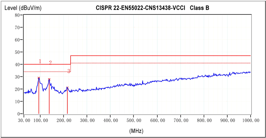
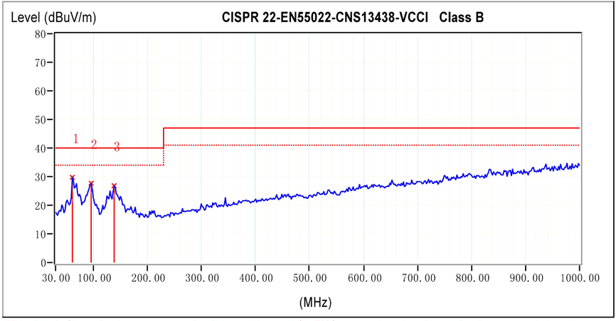
Figure 31 and Figure 32 are TPA3128D2 EN55022 Radiated Emissions results uses TPA3128D2EVM with 8-Ω speakers.
 Figure 31. TPA3128D2 Radiated Emissions-Horizontal (PVCC=12V, PO=1W)
 Figure 32. TPA3128D2 Radiated Emissions-Vertical (PVCC=12V, PO=1W)