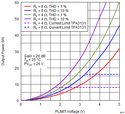
-
TPA313xD2 4-W, 25-W Filter-Free Class-D Stereo Amplifier With AM Avoidance
- 1 Features
- 2 Applications
- 3 Description
- 4 Revision History
- 5 Pin Configuration and Functions
- 6 Specifications
-
7 Detailed Description
- 7.1 Overview
- 7.2 Functional Block Diagram
- 7.3
Feature Description
- 7.3.1 Gain Setting and Master and Slave
- 7.3.2 Input Impedance
- 7.3.3 Start-up/Shutdown Operation
- 7.3.4 PLIMIT Operation
- 7.3.5 GVDD Supply
- 7.3.6 BSPx and BSNx Capacitors
- 7.3.7 Differential Inputs
- 7.3.8 Device Protection System
- 7.3.9 DC Detect Protection
- 7.3.10 Short-Circuit Protection and Automatic Recovery Feature
- 7.3.11 Thermal Protection
- 7.3.12 Efficiency: LC Filter Required with the Traditional Class-D Modulation Scheme
- 7.3.13 Ferrite Bead Filter Considerations
- 7.3.14 When to Use an Output Filter for EMI Suppression
- 7.3.15 AM Avoidance EMI Reduction
- 7.4 Device Functional Modes
- 8 Applications and Implementation
- 9 Power Supply Recommendations
- 10Layout
- 11Device and Documentation Support
- 12Mechanical, Packaging, and Orderable Information
- IMPORTANT NOTICE
パッケージ・オプション
メカニカル・データ(パッケージ|ピン)
- RHB|32
サーマルパッド・メカニカル・データ
- RHB|32
発注情報
TPA313xD2 4-W, 25-W Filter-Free Class-D Stereo Amplifier With AM Avoidance
1 Features
- Supports Multiple Output Configurations
- 2 × 4 W into a 8-Ω BTL Load at 7.4 V (TPA3131D2)
- 2 × 25 W into a 8-Ω BTL Load at 19 V (TPA3132D2)
- Wide Voltage Range: 4.5 V to 26 V
- Automotive Load-Dump Compliant
- Efficient Class-D Operation
- >90% Power Efficiency Combined With Low Idle Loss for Heat Sink free Operation
- Advanced Modulation Schemes
- Multiple Switching Frequencies
- AM Avoidance
- Master and Slave Synchronization
- Up to 1.2-MHz Switching Frequency
- Feedback Power Stage Architecture With High PSRR Reduces PSU Requirements
- Programmable Power Limit
- Differential and Single-Ended Inputs
- Stereo and Mono Mode With Single-Filter Mono Configuration
- Single Power Supply Reduces Component Count
- Integrated Self-Protection Circuits Including Overvoltage, Undervoltage, Overtemperature, DC-Detect, and Short Circuit With Error Reporting
- Thermally Enhanced Package
- 32-Pin VQFN Pad-Down
- –40°C to 85°C Ambient Temperature Range
2 Applications
- Laptop Computers and Ultrabooks
- Flatpanel TV
- Consumer Audio Applications
3 Description
The TPA313xD2 are efficient, stereo digital amplifier power stages for driving speakers with up to 2x42W/4Ω peak power. TPA3131/32D2 operates heatsink-free with cooling to PCB through the bottom side PowerPAD™ with sustained output power from 2 × 4 W / 8 Ω (TPA3131D2) to 2 × 25 W / 8 Ω (TPA3132D2).
The TPA313xD2 advanced oscillator/PLL circuit employs a multiple switching frequency option to avoid AM interferences; this is achieved together with an option of Master and Slave synchronization, making it possible to synchronize multiple devices.
The TPA313xD2 are fully protected against faults with short-circuit protection and thermal protection as well as overvoltage, undervoltage, and DC protection. Faults are reported back to the processor to prevent devices from being damaged during overload conditions.
For feature compatible devices see: PowerPAD up device 2 × 50-W TPA3116D2, PowerPAD down 2 × 15-W TPA3130D2 and 2 × 30-W TPA3118D2.
Device Information(1)
| PART NUMBER | PACKAGE | BODY SIZE (NOM) |
|---|---|---|
| TPA3131D2 | VQFN (32) | 5.00 mm × 5.00 mm |
| TPA3132D2 |
- For all available packages, see the orderable addendum at the end of the datasheet.
Simplified Application Circuit
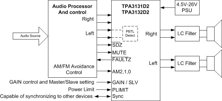
4 Revision History
Changes from A Revision (September 2013) to B Revision
- Added Pin Configuration and Functions section, ESD Ratings table, Feature Description section, Device Functional Modes, Application and Implementation section, Power Supply Recommendations section, Layout section, Device and Documentation Support section, and Mechanical, Packaging, and Orderable Information section Go
- Changed Gain (BTL) to Gain (MSTR)Go
- Changed Gain (MSTR) R1 values to R2 values and R2 values to R1 valuesGo
- Changed Gain (SLV) R1 values to R2 values and R2 values to R1 valuesGo
- Deleted BD Mode from TYPICAL CHARACTERISTICS conditionsGo
- Changed legends in Figure 13Go
5 Pin Configuration and Functions
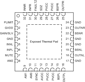
Pin Functions
| PIN | TYPE(1) | DESCRIPTION | |
|---|---|---|---|
| NO. | NAME | ||
| 1 | PLIMIT | I | Power limit level adjust. Connect a resistor divider from GVDD to GND to set power limit. Connect directly to GVDD for no power limit. |
| 2 | GVDD | PO | Internally generated gate voltage supply. Not to be used as a supply or connected to any component other than a 1uF X7R ceramic decoupling capacitor. |
| 3 | GAIN/SLV | I | Sets Gain and selects between Master and Slave mode depending on pin voltage divider. |
| 4 | GND | G | Ground |
| 5 | INNL | I | Negative audio input for left channel. Biased at 3V. |
| 6 | INPL | I | Positive audio input for left channel. Biased at 3V. |
| 7 | MUTE | I | Mute signal for fast disable/enable of outputs: HIGH = outputs OFF (high-Z), LOW = outputs ON. TTL logic levels with compliance to AVCC. |
| 8 | AM2 | I | AM Avoidance Frequency Selection |
| 9 | AM1 | I | AM Avoidance Frequency Selection |
| 10 | AM0 | I | AM Avoidance Frequency Selection |
| 11 | SYNC | DIO | Clock input/output for synchronizing multiple class-D devices. Direction determined by GAIN/SLV pin. Input signal not to exceed GVDD (7V) |
| 12 | AVCC | P | Analog Supply |
| 13 | PVCC | P | Power supply |
| 14 | PVCC | P | Power supply |
| 15 | BSPL | BST | Boot strap for positive left channel output, connect to 220nF X7R ceramic cap to OUTPL |
| 16 | OUTPL | PO | Positive left channel output |
| 17 | GND | G | Ground |
| 18 | OUTNL | PO | Negative left channel output |
| 19 | BSNL | BST | Boot strap for negative left channel output, connect to 220nF X7R ceramic cap to OUTNL |
| 20 | GND | G | Ground |
| 21 | GND | G | Ground |
| 22 | BSNR | BST | Boot strap for negative right channel output, connect to 220nF X7R ceramic cap to OUTNR |
| 23 | OUTNR | PO | Negative right channel output |
| 24 | GND | G | Ground |
| 25 | OUTPR | PO | Positive right channel output |
| 26 | BSPR | BST | Boot strap for positive right channel output, connect to 220nF X7R ceramic cap to OUTPR |
| 27 | PVCC | PI | Power supply |
| 28 | PVCC | PI | Power supply |
| 29 | SDZ | I | Shutdown logic input for audio amp (LOW = outputs Hi-Z, HIGH = outputs enabled). TTL logic levels with compliance to AVCC. |
| 30 | FAULTZ | DO | General fault reporting including Over-current_PVCC, OVP_DVDD FAULT1Z = High, normal operation FAULT1Z = Low, fault condition |
| 31 | INPR | I | Positive audio input for right channel. Biased at 3V. |
| 32 | INNR | I | Negative audio input for right channel. Biased at 3V. |
| 33 | Thermal pad | G | Connect to GND for best system performance. If not connected to GND, leave floating. |
6 Specifications
6.1 Absolute Maximum Ratings
over operating free-air temperature range (unless otherwise noted)| MIN | MAX | UNIT | ||
|---|---|---|---|---|
| Supply voltage, VCC | PVCC, AVCC | –0.3 | 30 | V |
| Input voltage, VI | INPL, INNL, INPR, INNR | –0.3 | 6.3 | V |
| PLIMIT, GAIN / SLV, SYNC | –0.3 | GVDD+0.3 | V | |
| AM0, AM1, AM2, MUTE, SDZ | –0.3 | PVCC+0.3 | V | |
| Slew rate, maximum | AM0, AM1, AM2, MUTE, SDZ | 10 | V/ms | |
| Operating free-air temperature, TA | –40 | 85 | °C | |
| Operating junction temperature, TJ | –40 | 150 | °C | |
| Storage temperature, Tstg | –40 | 125 | °C | |
6.2 ESD Ratings
| VALUE | UNIT | |||
|---|---|---|---|---|
| V(ESD) | Electrostatic discharge | Human-body model (HBM), per ANSI/ESDA/JEDEC JS-001(1) | ±2000 | V |
| Charged-device model (CDM), per JEDEC specification JESD22-C101(2) | ±500 | |||
6.3 Recommended Operating Conditions
over operating free-air temperature range (unless otherwise noted)| MIN | NOM | MAX | UNIT | ||||
|---|---|---|---|---|---|---|---|
| VCC | Supply voltage | PVCC, AVCC | 4.5 | 26 | V | ||
| VIH | High-level input voltage | AM0, AM1, AM2, MUTE, SDZ, SYNC | 2 | V | |||
| VIL | Low-level input voltage | AM0, AM1, AM2, MUTE, SDZ, SYNC | 0.8 | V | |||
| VOL | Low-level output voltage | FAULTZ, RPULL-UP = 100 kΩ, PVCC = 26 V | 0.8 | V | |||
| IIH | High-level input current | AM0, AM1, AM2, MUTE, SDZ (VI = 2 V, VCC = 18 V) | 50 | µA | |||
| RL(BTL) | Minimum load Impedance | Output filter: L = 10 µH, C = 680 nF | 3.2 | 4 | Ω | ||
| RL(PBTL) | Output filter: L = 10 µH, C = 1 µF | 1.6 | |||||
| Lo | Output-filter Inductance | Minimum output filter inductance under short-circuit condition | 1 | µH | |||
6.4 Thermal Information
| THERMAL METRIC(1)(2) | TPA313xD2 | UNIT | ||
|---|---|---|---|---|
| VQFN | ||||
| 32 PINS | ||||
| RθJA | Junction-to-ambient thermal resistance | 31.3 | °C/W | |
| ψJT | Junction-to-top characterization parameter | 0.2 | ||
| ψJB | Junction-to-board characterization parameter | 5.5 | ||
6.5 DC Electrical Characteristics
TA = 25°C, AVCC = PVCC = 7.4 V to 26 V, RL = 8 Ω (unless otherwise noted)6.6 AC Electrical Characteristics
TA = 25°C, AVCC = PVCC = 7.4 V to 24 V, RL = 8 Ω (unless otherwise noted)| PARAMETER | TEST CONDITIONS | MIN | TYP | MAX | UNIT | |
|---|---|---|---|---|---|---|
| KSVR | Power supply ripple rejection | 200 mVPP ripple at 1 kHz, Gain = 20 dB, Inputs AC-coupled to GND | –70 | dB | ||
| PO | Continuous output power | RL = 8 Ω, THD+N = 10%, f = 1 kHz, PVCC = 7.4 V (TPA3131D2) | 4 | W | ||
| RL = 4 Ω, THD+N = 10%, f = 1 kHz, PVCC = 7.4 V (TPA3131D2) | 7.3 | |||||
| RL = 8 Ω, THD+N = 10%, f = 1 kHz, PVCC = 19V (TPA3132D2) | 25 | |||||
| RL = 4 Ω, THD+N = 10%, f = 1 kHz, PVCC = 19V (TPA3132D2) | 42 | |||||
| THD+N | Total harmonic distortion + noise | RL = 8 Ω, f = 1 kHz, PO = 0.1W to 2 W (TPA3132D2) RL = 8 Ω, f = 1 kHz, PO = 0.1W to 12.5 W (TPA3131D2) |
0.1% | |||
| Vn | Output integrated noise | 20 Hz to 22 kHz, A-weighted filter, Gain = 20 dB | 70 | µV | ||
| –80 | dBV | |||||
| Crosstalk | VO = 1 Vrms, Gain = 20 dB, f = 1 kHz | –100 | dB | |||
| SNR | Signal-to-noise ratio | Maximum output at THD+N < 1%, f = 1 kHz, Gain = 20 dB, A-weighted (TPA3131D2, PVCC = 7.4V) | 98 | dB | ||
| Maximum output at THD+N < 1%, f = 1 kHz, Gain = 20 dB, A-weighted (TPA3131D2, PVCC = 19V) | 105 | |||||
| fOSC | Oscillator frequency | AM2=0, AM1=0, AM0=0 | 376 | 400 | 424 | kHz |
| AM2=0, AM1=0, AM0=1 | 470 | 500 | 530 | |||
| AM2=0, AM1=1, AM0=0 | 564 | 600 | 636 | |||
| AM2=0, AM1=1, AM0=1 | 940 | 1000 | 1060 | |||
| AM2=1, AM1=0, AM0=0 | 1128 | 1200 | 1278 | |||
| AM2=1, AM1=0, AM0=1 | Reserved | |||||
| AM2=1, AM1=1, AM0=0 | ||||||
| AM2=1, AM1=1, AM0=1 | ||||||
| Thermal trip point | 150+ | °C | ||||
| Thermal hysteresis | 15 | °C | ||||
| Over current trip point | TPA3131D2 | 3.4 | A | |||
| TPA3132D2 | 7 | |||||
6.7 Typical Characteristics
fs = 400 kHz (unless otherwise noted)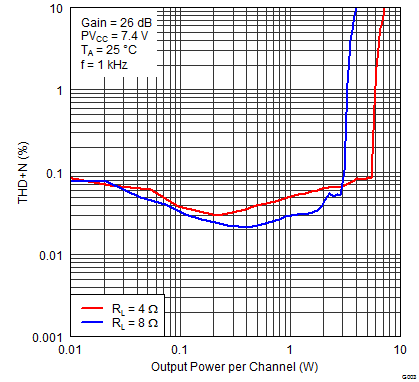 Figure 1. Total Harmonic Distortion + Noise (BTL) vs Output Power
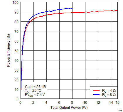 Figure 3. Power Efficiency (BTL) vs Supply Voltage
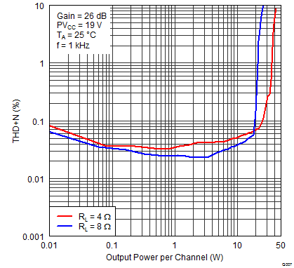 Figure 5. Total Harmonic Distortion + Noise (BTL) vs Output Power
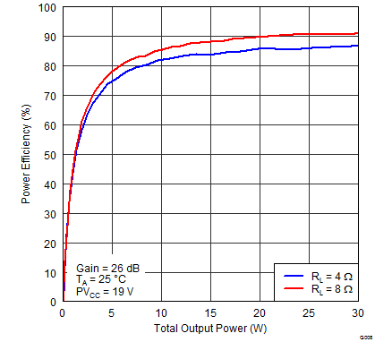 Figure 7. Power Efficiency (BTL) vs Output Power
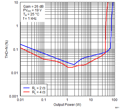 Figure 9. Total Harmonic Distortion + Noise (TPA3132D2 PBTL) vs Output Power
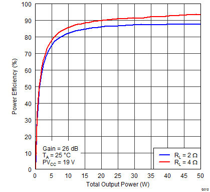 Figure 11. Power Efficiency (TPA3132D2 PBTL) vs Output Power
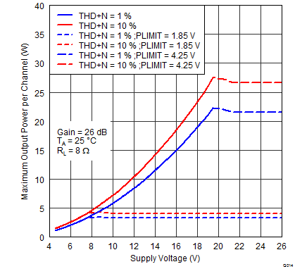 Figure 15. Maximum Output Power (BTL) vs Supply Voltage
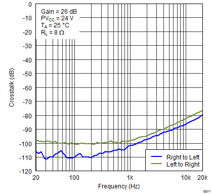 Figure 17. Crosstalk (BTL) vs Frequency
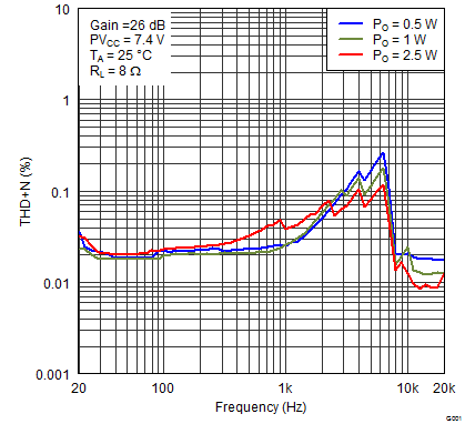 Figure 2. Total Harmonic Distortion + Noise (BTL) vs Frequency
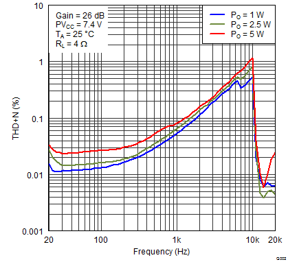 Figure 4. Total Harmonic Distortion + Noise (BTL) vs Frequency
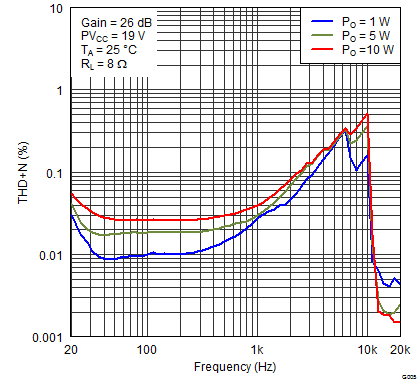 Figure 6. Total Harmonic Distortion + Noise (BTL) vs Frequency
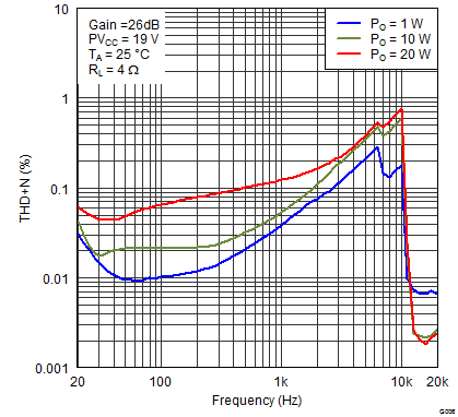 Figure 8. Total Harmonic Distortion + Noise (BTL) vs Frequency
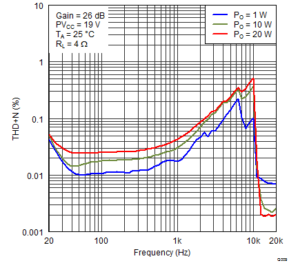 Figure 10. Total Harmonic Distortion + Noise (TPA3132D2 PBTL) vs Frequency
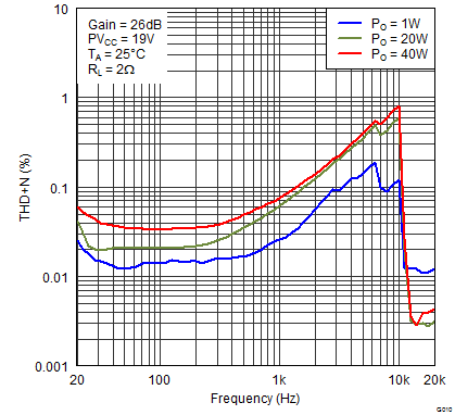 Figure 12. Total Harmonic Distortion + Noise (TPA3132D2 PBTL) vs Frequency
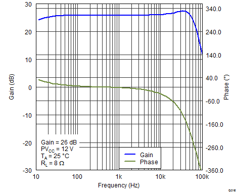 Figure 14. Gain/Phase (BTL) vs Frequency
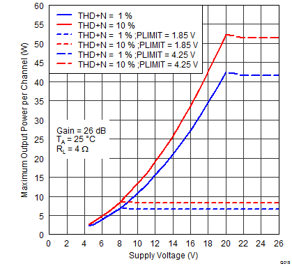 Figure 16. Maximum Output Power (BTL) vs Supply Voltage
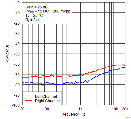 Figure 18. PSRR vs Frequency
