JAJSC84F May 2016 – January 2020 TPA3136AD2 , TPA3136D2
PRODUCTION DATA.
- 1 特長
- 2 アプリケーション
- 3 概要
- 4 改訂履歴
- 5 概要(続き)
- 6 Device Comparison Table
- 7 Pin Configuration and Functions
- 8 Specifications
- 9 Parameter Measurement Information
- 10Detailed Description
-
11Application and Implementation
- 11.1 Application Information
- 11.2
Typical Applications
- 11.2.1 Design Requirements
- 11.2.2
Detailed Design Procedure
- 11.2.2.1 Ferrite Bead Filter Considerations
- 11.2.2.2 Efficiency: LC Filter Required with the Traditional Class-D Modulation Scheme
- 11.2.2.3 When to Use an Output Filter for EMI Suppression
- 11.2.2.4 Input Resistance
- 11.2.2.5 Input Capacitor, Ci
- 11.2.2.6 BSN and BSP Capacitors
- 11.2.2.7 Differential Inputs
- 11.2.2.8 Using Low-ESR Capacitors
- 11.2.3 Application Performance Curves
- 12Power Supply Recommendations
- 13Layout
- 14デバイスおよびドキュメントのサポート
- 15メカニカル、パッケージ、および注文情報
パッケージ・オプション
メカニカル・データ(パッケージ|ピン)
- PWP|28
サーマルパッド・メカニカル・データ
- PWP|28
発注情報
11.2.2.3 When to Use an Output Filter for EMI Suppression
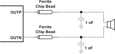
The TPA3136D2 device has been tested with a simple ferrite bead filter for a variety of applications including long speaker wires up to 100 cm and high power. The TPA3136D2 EVM passes FCC Class B specifications under these conditions using twisted speaker wires. The size and type of ferrite bead can be selected to meet application requirements. Also, the filter capacitor can be increased if necessary with some impact on efficiency.
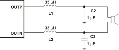
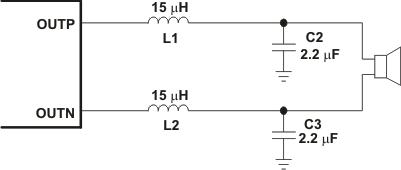
There may be a few circuit instances where it is necessary to add a complete LC reconstruction filter. These circumstances might occur if there are nearby circuits which are sensitive to noise. In these cases, a classic second order Butterworth filter similar to those shown in the following figures can be used.
Some systems have little power supply decoupling from the AC line, but are also subject to line conducted interference (LCI) regulations. These include systems powered by "wall warts" and "power bricks." In these cases, LC reconstruction filters can be the lowest cost means to pass LCI tests. Common mode chokes using low frequency ferrite material can also be effective at preventing line conducted interference.
 Figure 20. Typical Ferrite Chip Bead Filter (Chip Bead Example: NFZ2MSM series from Murata)
  Figure 21. Typical LC Output Filter, Cutoff Frequency of 27 kHz, Speaker Impedance = 8 Ω
  Figure 22. Typical LC Output Filter, Cutoff Frequency of 27 kHz, Speaker Impedance = 6 Ω