JAJSI28A October 2019 – August 2020 TPA3139D2
PRODUCTION DATA
- 1 特長
- 2 アプリケーション
- 3 概要
- 4 Revision History
- 5 Pin Configuration and Functions
- 6 Specifications
-
7 Detailed Description
- 7.1 Overview
- 7.2 Functional Block Diagram
- 7.3
Feature Description
- 7.3.1 Analog Gain
- 7.3.2 SD/ FAULT and MUTE Operation
- 7.3.3 PLIMIT
- 7.3.4 Spread Spectrum and De-Phase Control
- 7.3.5 GVDD Supply
- 7.3.6 DC Detect
- 7.3.7 PBTL Select
- 7.3.8 Short-Circuit Protection and Automatic Recovery Feature
- 7.3.9 Over-Temperature Protection (OTP)
- 7.3.10 Over-Voltage Protection (OVP)
- 7.3.11 Under-Voltage Protection (UVP)
- 7.4 Device Functional Modes
-
8 Application and Implementation
- 8.1 Application Information
- 8.2
Typical Applications
- 8.2.1 Design Requirements
- 8.2.2
Detailed Design Procedure
- 8.2.2.1 Ferrite Bead Filter Considerations
- 8.2.2.2 Efficiency: LC Filter Required with the Traditional Class-D Modulation Scheme
- 8.2.2.3 When to Use an Output Filter for EMI Suppression
- 8.2.2.4 Input Resistance
- 8.2.2.5 Input Capacitor, Ci
- 8.2.2.6 BSN and BSP Capacitors
- 8.2.2.7 Differential Inputs
- 8.2.2.8 Using Low-ESR Capacitors
- 8.2.3 Application Performance Curves
- 9 Power Supply Recommendations
- 10Layout
- 11Device and Documentation Support
パッケージ・オプション
メカニカル・データ(パッケージ|ピン)
- RGE|24
サーマルパッド・メカニカル・データ
- RGE|24
発注情報
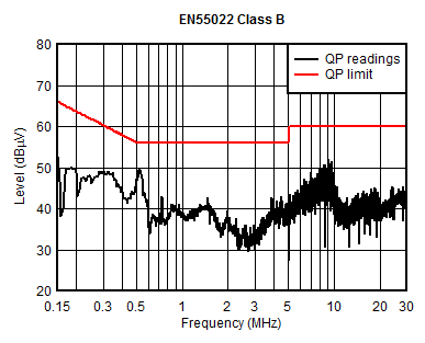
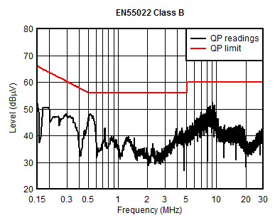
8.2.3.2 EN55022 Conducted Emissions Results
TPA3139D2 EVM, PVCC = 12 V, 8-Ω speakers, PO = 4 W
TPA3139D2 EVM, PVCC = 12 V, 8-Ω speakers, PO = 4 W Figure 8-8 Conducted Emission - Line. TPA3139D2 EVM, PVCC = 12 V, 8-Ω speakers, PO = 4 W
 Figure 8-8 Conducted Emission - Line. TPA3139D2 EVM, PVCC = 12 V, 8-Ω speakers, PO = 4 W
 Figure 8-9 Conducted Emission - Neutral