JAJSE46B September 2017 – December 2017 TPA3221
PRODUCTION DATA.
- 1 特長
- 2 アプリケーション
- 3 概要
- 4 改訂履歴
- 5 Device Comparison Table
- 6 Pin Configuration and Functions
-
7 Specifications
- 7.1 Absolute Maximum Ratings
- 7.2 ESD Ratings
- 7.3 Recommended Operating Conditions
- 7.4 Thermal Information
- 7.5 Electrical Characteristics
- 7.6 Audio Characteristics (BTL)
- 7.7 Audio Characteristics (PBTL)
- 7.8 Typical Characteristics, BTL Configuration, AD-mode
- 7.9 Typical Characteristics, PBTL Configuration, AD-mode
- 8 Parameter Measurement Information
-
9 Detailed Description
- 9.1 Overview
- 9.2 Functional Block Diagrams
- 9.3 Feature Description
- 9.4
Device Functional Modes
- 9.4.1 Powering Up
- 9.4.2 Powering Down
- 9.4.3 Device Reset
- 9.4.4 Device Soft Mute
- 9.4.5
Device Protection System
- 9.4.5.1 Overload and Short Circuit Current Protection
- 9.4.5.2 Signal Clipping and Pulse Injector
- 9.4.5.3 DC Speaker Protection
- 9.4.5.4 Pin-to-Pin Short Circuit Protection (PPSC)
- 9.4.5.5 Overtemperature Protection OTW and OTE
- 9.4.5.6 Undervoltage Protection (UVP), Overvoltage Protection (OVP) and Power-on Reset (POR)
- 9.4.5.7 Fault Handling
- 10Application and Implementation
- 11Power Supply Recommendations
- 12Layout
- 13デバイスおよびドキュメントのサポート
- 14メカニカル、パッケージ、および注文情報
パッケージ・オプション
メカニカル・データ(パッケージ|ピン)
- DDV|44
サーマルパッド・メカニカル・データ
- DDV|44
発注情報
9 Detailed Description
9.1 Overview
TPA3221 is designed as a feature-enhanced cost efficient high power Class-D audio amplifier. It has built-in advanced protection circuitry to ensure maximum product robustness as well as a flexible feature set including built in LDO for easy supply of low voltage circuitry, selectable gain, switching frequency, master/slave synchronization of multiple devices, selectable PWM modulation scheme, mute function, temperature and clipping status signals. TPA3221 has a bandwidth up to 100 kHz and low output noise designed for high resolution audio applications and accepts both differential and single ended analog audio inputs at levels from 1 VRMS to 2 VRMS. With its closed loop operation TPA3221 is designed for high audio performance with a system power supply between 7 V and 30 V.
To facilitate system design, the TPA3221 needs only a (typical) 30 V power stage supply. The TPA3221 has an internal voltage regulator supplied from the VDD pin for the analog and digital system blocks and the output stage gate drive respectively. The VDD pin can be connected directly to PVDD in case of only this power supply rail available.
To reduce device power losses external 5 V supplies can be used for the AVDD and VDD supply pins. The internal voltage regulator connected to the VDD pin is automatically turned off if using external 5 V supply for this pin. Although supplied from the same 5 V source, separating AVDD and VDD on the printed-circuit board (PCB) by RC filters (see application diagram for details) is recommended. These RC filters provide the recommended high-frequency isolation. Special attention should be paid to placing all decoupling capacitors as close to their associated pins as possible. In general, the physical loop with the power supply pins, decoupling capacitors and GND return path to the device pins must be kept as short as possible and with as little area as possible to minimize induction (see Layout Examples for additional information).
The floating supplies for the output stage high side gate drives are supplied by built-in bootstrap circuitry requiring only an external capacitor for each half-bridge.
For a properly functioning bootstrap circuit, a small ceramic capacitor must be connected from each bootstrap pin (BST_X) to the power-stage output pin (OUT_X). When the power-stage output is low, the bootstrap capacitor is charged through an internal diode connected between the gate-drive power-supply pin (GVDD) and the bootstrap pins. When the power-stage output is high, the bootstrap capacitor potential is shifted above the output potential and thus provides a suitable voltage supply for the high-side gate driver. It is recommended to use 33 nF ceramic capacitors, size 0603 or 0805, for the bootstrap supply. These 33 nF capacitors ensure sufficient energy storage, even during minimal PWM duty cycles, to keep the high-side power stage FET (LDMOS) fully turned on during the remaining part of the PWM cycle.
Special attention should be paid to the power stage power supply; this includes component selection, PCB placement, and routing.
For optimal electrical performance, EMI compliance, and system reliability, it is important that each PVDD_X node is decoupled with 1 μF ceramic capacitors placed as close as possible to the PVDD supply pins. It is recommended to follow the PCB layout of the TPA3221 reference design. For additional information on recommended power supply and required components, see the application diagrams in this data sheet.
If using external power supply for the AVDD and VDD internal regulators, this supply should be from a low-noise, low-output-impedance voltage regulator. Likewise, the 30 V power stage supply is assumed to have low output impedance throughout the entire audio band, and low noise. The power supply sequence is not critical as facilitated by the internal power-on-reset circuit, but it is recommended to release RESET after the power supply is settled for minimum turn on audible artefacts. Moreover, the TPA3221 is fully protected against erroneous power-stage turn on due to parasitic gate charging. Thus, voltage-supply ramp rates (dV/dt) are noncritical within the specified range (see the Recommended Operating Conditions table of this data sheet).
9.2 Functional Block Diagrams
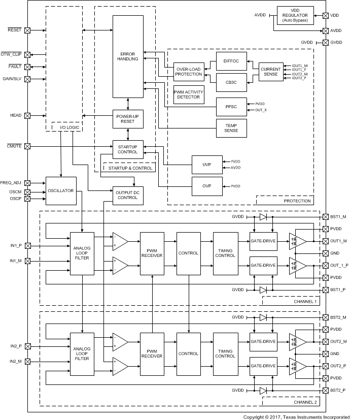
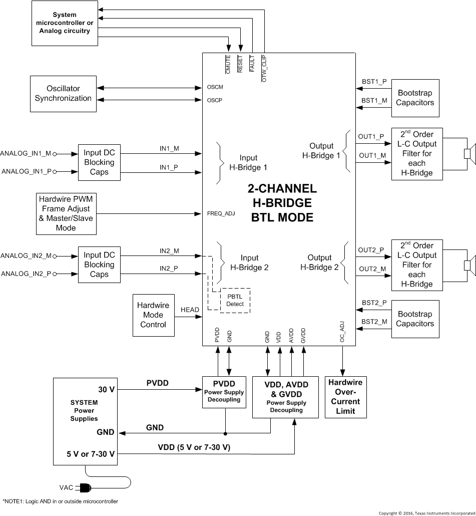 Figure 27. System Block Diagram
9.3 Feature Description
9.3.1 Internal LDO
TPA3221 has a built in optional LDO (Low dropout voltage regulator) to supply the analog and digital circuits as well as the gate drive for the output stages. The LDO can be used in systems where only the high voltage power rail is available, hence no additional power supply rails need to be generated for the TPA3221 to operate. As being a linear regulator, the LDO will add to the power losses of the device due to the (PVDD-5V) voltage drop and the supply current for AVDD and GVDD given in the Electrical Characteristics table.
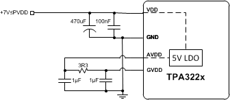 Figure 28. Internal LDO for Single Supply Systems
When using the internal LDO in TPA3221 the VDD terminal should be connected to a voltage source between 7V and PVDD. In a single supply system the VDD terminal should be connected directly to the PVDD terminal. The LDO output is connected to the AVDD terminal, and can be used to supply the gate drive by supplying the GVDD from AVDD through a RC filter for best noise performance as shown in Figure 28.
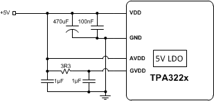 Figure 29. Internal LDO Bypass for Highest Power Efficiency
For highest system power efficiency the LDO can be bypassed by connecting VDD to an external 5 V supply. In this configuration AVDD and GVDD should be supplied by 5 V from the external power supply. GVDD should be supplied through a RC filter for best noise performance as shown in Figure 29.
9.3.1.1 Input Configuration, Gain Setting And Master / Slave Operation
TPA3221 is designed to accept either a differential or a single-ended audio input signal. To accept a wide range of system front ends TPA3221 has selectable input gain that allows full scale output with a wide range of input signal levels.
Best system noise performance is obtained with balanced audio interface. However, to be used in systems with only a single ended audio input signal available, one input terminal can be connected to AC ground, to accept single ended audio input signals.
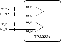 Figure 30. Balanced Audio Input Configuration
In systems with single ended audio inputs the device gain will typically need to be set higher than for systems with balanced audio input signals.
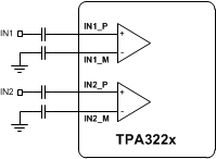 Figure 31. Single Ended Audio Input Configuration
9.3.2 Gain Setting And Master / Slave Operation
The gain of TPA3221 is set by the voltage divider connected to the GAIN/SLV control pin. Master or Slave mode is also controlled by the same pin. An internal ADC is used to detect the 8 input states. The first four stages sets the GAIN in Master mode in gains of 18, 24, 30, 34 dB respectively, while the next four stages sets the GAIN in Slave mode in gains of 18, 24, 30, 34 dB respectively. The gain setting is latched when RESET goes high and cannot be changed while RESET is high. Table 2 shows the recommended resistor values, the state and gain:
Table 2. Gain and Master / Slave
| Master / Slave Mode | Gain | R1 (to GND) | R2 (to AVDD) | Differential Input Signal Level (each input pin) |
Single Ended Input Signal Level |
|---|---|---|---|---|---|
| Master | 18 dB | 5.6 kΩ | OPEN | 2 VRMS | 2 VRMS |
| Master | 24 dB | 20 kΩ | 100 kΩ | 1 VRMS | 2 VRMS |
| Master | 30 dB | 39 kΩ | 100 kΩ | 0.5 VRMS | 1 VRMS |
| Master | 34 dB | 47 kΩ | 75 kΩ | 0.32 VRMS | 0.63 VRMS |
| Slave | 18 dB | 51 kΩ | 51 kΩ | 2 VRMS | 2 VRMS |
| Slave | 24 dB | 75 kΩ | 47 kΩ | 1 VRMS | 2 VRMS |
| Slave | 30 dB | 100 kΩ | 39 kΩ | 0.5 VRMS | 1 VRMS |
| Slave | 34 dB | 100 kΩ | 16 kΩ | 0.32 VRMS | 0.63 VRMS |
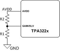 Figure 32. Gain and Master / Slave Setup
For easy multi-channel system design TPA3221 has a Master / Slave feature that allows automatic synchronization of multiple slave devices operated at the PWM switching frequency of a master device. This benefits system noise performance by eliminating spurious crosstalk sum and difference tones due to unsynchronized channel-to-channel switching frequencies. Furthermore the Master / Slave scheme is designed to interleave switching of the individual channels in a multi-channel system such that the power supply current ripple frequency is moved to a higher frequency which reduces the RMS ripple current in the power supply bulk capacitors.
The Master / Slave scheme and the interleaving of the output stage switching is automatically configured by connecting the OSCx pins between a master and multiple slave devices. Connect the OSCx pins in either positive or negative polarity to configure either a Slave1 or Slave2 device. Connect the OSCM of the Master device to the OSCM of a slave device to configure for Slave1 or OSCP to configure for Slave2. Then connect the remaining OSCx pins between the master and slave devices. The Master, Slave1 and Slave2 PWM switching will be 30 degrees out of phase with each other. All switching channels are automatically synchronized by releasing /RESET on all devices at the same time.
 Figure 33. Gain and Master PCB Implementation
Placement on the PCB and connection of multiple TPA3221 devices in a multi channel system is illustrated in Figure 33. Slave devices should be placed on either side of the master device, with a Slave1 device on one side of the Master device, and a Slave2 device on the other. In systems with more than 3 TPA3221 devices, the master should be in the middle, and every second slave devices should be a Slave1 or Slave 2 as illustrated in Figure 33. A 47kΩ pull up resistor to AVDD should be connected to the master device OSCM output and a 47kΩ pull down resistor to GND should be connected to the master OSCP CLK outputs.
9.3.3 AD-Mode and HEAD-Mode PWM Modulation
TPA3221 has the option of using either AD-Mode or HEAD-Mode PWM modulation scheme. AD mode has continuous switching of the two half bridge outputs in each BTL output channel. Both half bridge outputs are switching in HEAD mode, but with reduced duty cycle for idle operation and while playing small signals. With higher output levels one half bridge stops switching on HEAD mode operation. HEAD benefits both device power loss and EMI performance, where AD mode is considered to have the highest audio performance.
SPACE
 Figure 34. AD-Mode Configuration
 Figure 35. HEAD-Mode Configuration
 Figure 36. AD Mode Output Waveforms, Idle
 Figure 37. AD Mode Output Waveforms, High Level Output
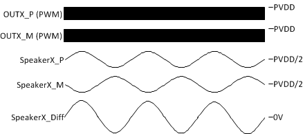 Figure 38. AD Mode Speaker Output Signals, Low or and High Level Output
 Figure 39. HEAD Mode Output Waveforms, Idle
 Figure 40. HEAD Mode Output Waveforms, High Level Output
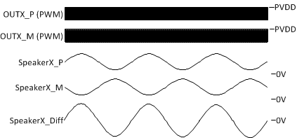 Figure 41. HEAD Mode Speaker Output Signals, Low Level Output
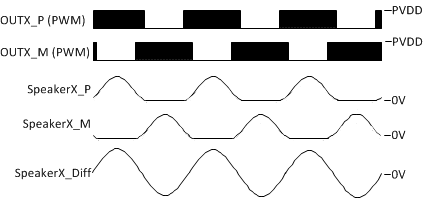 Figure 42. HEAD Mode Speaker Output Signals, High Level Output
9.3.4 Oscillator
The oscillator frequency can be trimmed by external control of the FREQ_ADJ pin.
To reduce interference problems while using radio receiver tuned within the AM band, the switching frequency can be changed from nominal to higher values. These values should be chosen such that the nominal and the higher value switching frequencies together results in the fewest cases of interference throughout the AM band. The oscillator frequency can be selected by the value of the FREQ_ADJ resistor connected to GND in master mode according to the description in the Recommended Operating Conditions table.
For slave mode operation, turn off the oscillator by pulling the FREQ_ADJ pin to AVDD. This configures the OSC_I/O pins as inputs to be slaved from an external differential clock. In a master/slave system inter channel delay is automatically setup between the switching of the audio channels, which can be illustrated by no idle channels switching at the same time. This will not influence the audio output, but only the switch timing to minimize noise coupling between audio channels through the power supply to optimize audio performance and to get better operating conditions for the power supply. The inter channel delay will be setup for a slave device depending on the polarity of the OSC_I/O connection such that a slave mode 1 is selected by connecting the master device OSC_I/O to the slave 1 device OSC_I/O with same polarity (+ to + and - to -), and slave mode 2 is selected with the inverse polarity (+ to - and - to +).
9.3.5 Input Impedance
The TPA3221 input stage is a fully differential input stage and the input impedance changes with the gain setting from 7.7 kΩ at 34 dB gain to 47 kΩ at 18 dB gain. Table 1 lists the values from min to max gain. The tolerance of the input resistor value is ±20 % so the minimum value will be higher than 6.2 kΩ. The inputs need to be AC-coupled to minimize the output DC-offset and ensure correct ramping of the output voltages during power-ON and power-OFF. The input ac-coupling capacitor together with the input impedance forms a high-pass filter with the following cut-off frequency:
If a flat bass response is required down to 20 Hz the recommended cut-off frequency is a tenth of that, 2 Hz. Table 3 lists the recommended ac-couplings capacitors for each gain step. If a -3 dB is accepted at 20 Hz 10 times lower capacitors can used – for example, a 1 μF can be used.
Table 3. Recommended Input AC-Coupling Capacitors
| Gain | Input Impedance | Input AC-Coupling Capacitance | Input High Pass Filter |
|---|---|---|---|
| 18 dB | 48 kΩ | 4.7 µF | 0.7 Hz |
| 24 dB | 24 kΩ | 10 µF | 0.7 Hz |
| 30 dB | 12 kΩ | 10 µF | 1.3 Hz |
| 34 dB | 7.7 kΩ | 10 µF | 2.1 Hz |
The input capacitors used should be a type with low leakage, like quality electrolytic, tantalum, film or ceramic. If a polarized type is used the positive connection should face such that the capacitor has a positive DC bias.
9.3.6 Error Reporting
The FAULT, and OTW_CLIP, pins are active-low, open-drain outputs. The FAULT function is for protection-mode signaling to a system-control device. Any fault resulting in device shutdown is signaled by the FAULT pin going low. Also, OTW_CLIP goes low when the device junction temperature exceeds 125°C (see Table 4).
Table 4. Error Reporting
| FAULT | OTW_CLIP | DESCRIPTION |
|---|---|---|
| 0 | 0 | Overtemperature (OTE), overload (OLP), undervoltage (UVP), or overvoltage (OVP). Junction temperature higher than 125°C (overtemperature warning) |
| 0 | 1 | Overload (OLP), undervoltage (UVP), or overvoltage (OVP). Junction temperature lower than 125°C |
| 1 | 0 | Junction temperature higher than 125°C (overtemperature warning) |
| 1 | 1 | Junction temperature lower than 125°C and no OLP or UVP faults (normal operation) |
Note that asserting RESET low forces the FAULT signal high, independent of faults being present. TI recommends monitoring the OTW_CLIP signal using the system microcontroller and responding to an overtemperature warning signal by turning down the volume to prevent further heating of the device resulting in device shutdown (OTE).
To reduce external component count, an internal pullup resistor to 3.3 V is provided on both FAULT and OTW_CLIP outputs.
9.4 Device Functional Modes
TPA3221 can be configured in either a stereo BTL (Bridge Tied Load) mode, mono BTL mode (only one output BTL channel active), or in a mono PBTL (Parallel Bridge Tied Load) mode. In PBTL mode the two output BTL channels are parallelled with double output current available. The parallelling of the two BTL outputs can be made either before the output LC filter, or after the output LC filter. For PBTL mode the audio performance will in general be higher when parallelling before the output LC filter, but parallelling after the LC output filter may be preferred in some systems.
See Table 1 for mode configuration setup.
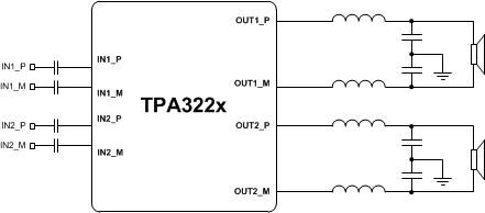 Figure 43. Stereo BTL
 Figure 45. Mono PBTL, Pre LC Filter
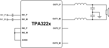 Figure 44. Mono BTL
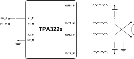 Figure 46. Mono PBTL, Post LC Filter
9.4.1 Powering Up
The TPA3221 does not require a power-up sequence because of the integrated undervoltage protection (UVP), but it is recommended to hold RESET low until PVDD supply voltage is stable to avoid audio artifacts. The outputs of the H-bridges remain in a high-impedance state until the gate-drive supply (GVDD) and AVDD voltages are above their UVP voltage thresholds (see the Electrical Characteristics table of this data sheet). This allows an internal circuit to charge the external bootstrap capacitors by enabling a weak pull-down of the half-bridge output as well as initiating a controlled ramp up sequence of the output voltage.
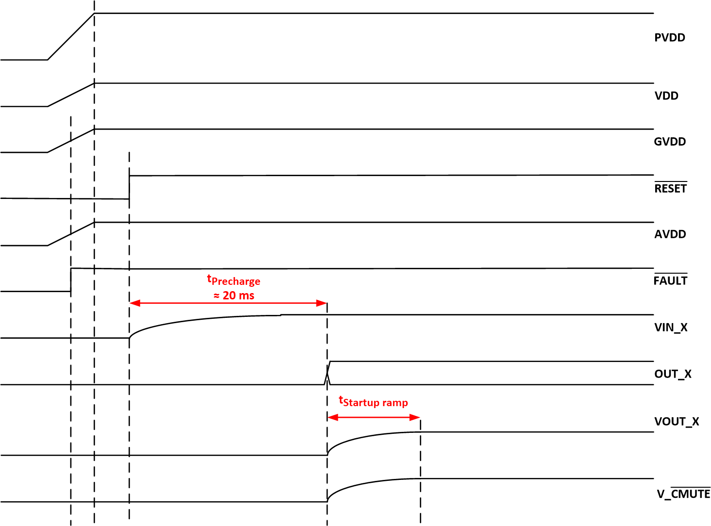 Figure 47. Startup Timing
When RESET is released to turn on TPA3221, FAULT signal will turn low and AVDD voltage regulator will be enabled. FAULT will stay low until AVDD reaches the undervoltage protection (UVP) voltage threshold (see the Electrical Characteristics table of this data sheet). After a pre-charge time to stabilize the DC voltage across the input AC coupling capacitors, the ramp up sequence starts and completes once the CMUTE node is charged to its final value.
9.4.1.1 Startup Ramp Time
During the startup ramp the CMUTE capacitor is charged by an internal current generator. With use of the recommended 33 nF CMUTE capacitor value, the startup ramp time is approximately 20 ms. Higher CMUTE capacitor value will increase the ramp time, and a lower value will decrease the ramp time. The recommended CMUTE capacitor value is selected for minimum audible artifacts during startup and shutdown ramp.
9.4.2 Powering Down
The TPA3221 does not require a power-down sequence. The device remains fully operational as long as the VDD, AVDD and PVDD voltages are above their undervoltage protection (UVP) voltage thresholds (see the Electrical Characteristics table of this data sheet). Although not specifically required, it is a good practice to hold RESET low during power down, thus preventing audible artifacts including pops or clicks by initiating a controlled ramp down sequence of the output voltage. The ramp down sequence will complete once the CMUTE node is discharged.
9.4.2.1 Power Down Ramp Time
During the power down ramp the CMUTE capacitor is discharged by internal circuitry. With use of the recommended 33 nF CMUTE capacitor value, the power-down ramp time is approximately 20 ms.
9.4.3 Device Reset
Asserting RESET low initiates the device ramp down. The output FETs go into a Hi-Z state after the ramp down is complete. Output pull downs are active in both BTL mode and PBTL mode with RESET low.
In BTL modes, to accommodate bootstrap charging prior to switching start, asserting the RESET input low enables weak pull-down of the half-bridge outputs.
Asserting RESET low removes any fault information to be signaled on the FAULT output, that is, FAULT is forced high. A rising-edge transition on RESET allows the device to resume operation after a fault. To ensure thermal reliability, the rising edge of RESET must occur no sooner than 4 ms after the falling edge of FAULT.
The TPA3221 will enter a low power state once the ramp down sequence is complete.
9.4.4 Device Soft Mute
Asserting CMUTE low initiates the device soft mute function. The soft mute function initiates a ramp down sequence of the outputs, and the output FETs go into a Hi-Z state after the ramp down is complete. All internal circuits are powered while in soft mute state. External control of the soft mute function must provide high impedance output when not engaged (open drain output) to allow the CMUTE node to charge/discharge during device ramp up and ramp down when de-asserting and asserting RESET.
9.4.5 Device Protection System
The TPA3221 contains advanced protection circuitry carefully designed to facilitate system integration and ease of use, as well as to safeguard the device from permanent failure due to a wide range of fault conditions such as short circuits, overload, overtemperature, overvoltage and undervoltage. The TPA3221 responds to a fault by immediately setting the power stage in a high-impedance (Hi-Z) state and asserting the FAULT pin low. In situations other than overload and overtemperature error (OTE), the device automatically recovers when the fault condition has been removed, that is, the supply voltage has increased. The device will handle errors, as shown in Table 5.
Table 5. Device Protection
| BTL MODE | PBTL MODE | ||
|---|---|---|---|
| LOCAL ERROR IN | TURNS OFF | LOCAL ERROR IN | TURNS OFF |
| A | A+B | A | A+B+C+D |
| B | B | ||
| C | C+D | C | |
| D | D | ||
Bootstrap UVP does not shutdown according to the table, it shuts down the respective halfbridge (non-latching, does not assert FAULT).
9.4.5.1 Overload and Short Circuit Current Protection
TPA3221 has fast reacting current sensors on all high-side and low-side FETs. To prevent output current from increasing beyond the overcurrent threshold, TPA3221 uses current limiting of the output current for each switching cycle (Cycle By Cycle Current Control, CB3C) in case of excess output current. CB3C prevents premature shutdown due to high output current transients caused by high level music transients and a drop of real speaker’s load impedance, and allows the output current to be limited to a maximum programmed level. If the maximum output current persists, i.e. the power stage being overloaded with too low load impedance, the device will shut down the affected output channel and the affected output is put in a high-impedance (Hi- Z) state until a RESET cycle is initiated. CB3C works individually for each full-bridge output. If an over current event is triggered, CB3C performs a state flip of the full-bridged output that is cleared upon beginning of next PWM frame.
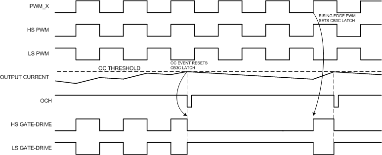 Figure 48. CB3C Timing Example
9.4.5.2 Signal Clipping and Pulse Injector
A built in activity detector monitors the PWM activity of the OUT_X pins. TPA3221 is designed to drive unclipped output signals all the way to PVDD and GND rails. In case of audio signal clipping when applying excessive input signal voltage, or in case of CB3C current protection being active, the amplifier feedback loop of the audio channel will respond to this condition with a saturated state, and the output PWM signals will stop unless special circuitry is implemented to handle this situation. To prevent the output PWM signals from stopping in a clipping or CB3C situation, narrow pulses are injected to the gate drive to maintain output activity. The injected narrow pulses are injected at every 4th PWM frame, and thus the effective switching frequency during this state is reduced to 1/4 of the normal switching frequency.
Signal clipping is signalled on the OTW_CLIP pin and is self clearing when signal level reduces and the device reverts to normal operation. The OTW_CLIP pulses starts at the onset to output clipping, typically at a THD level around 0.01%, resulting in narrow OTW_CLIP pulses starting with a pulse width of ~500ns.
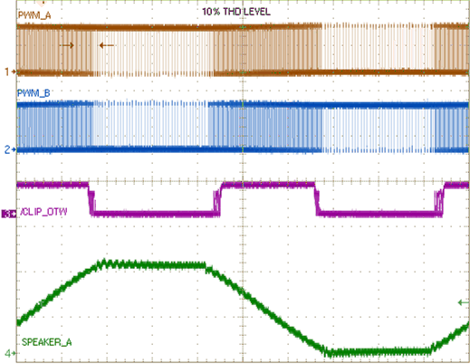 Figure 49. Signal Clipping PWM and Speaker Output Signals
9.4.5.3 DC Speaker Protection
The output DC protection scheme protects a speaker from excess DC current in case one terminal of the speaker is connected to the amplifier while the other is accidentally shorted to the chassis ground. Such a short circuit results in a DC voltage of PVDD/2 across the speaker, which potentially can result in destructive current levels. The output DC protection detects any unbalance of the output and input current of a BTL or PBTL output configuration (current into/out of one half-bridge equals current out of/into the other half-bridge), and in the event of the unbalance exceeding a programmed threshold, the overload counter increments until its maximum value and the affected output channel is shut down. DC Speaker Protection is enabled in both BTL and PBTL mode operation.
9.4.5.4 Pin-to-Pin Short Circuit Protection (PPSC)
The PPSC detection system protects the device from permanent damage in the case that a power output pin (OUT_X) is shorted to GND_X or PVDD_X. For comparison, the OC protection system detects an overcurrent after the demodulation filter where PPSC detects shorts directly at the pin before the filter. PPSC detection is performed at startup after RESET is pulled high. When PPSC detection is activated by a short on the output, all half-bridges are kept in a Hi-Z state until the short is removed; the device then continues the startup sequence and starts switching. The detection is controlled globally by a two step sequence. The first step ensures that there are no shorts from OUT_X to GND_X, the second step tests that there are no shorts from OUT_X to PVDD_X. The total duration of this process is roughly proportional to the capacitance of the output LC filter. The typical duration is < 15 ms/μF. While the PPSC detection is in progress, FAULT is kept low. If no shorts are present the PPSC detection passes, and FAULT is released. A device reset will start a new PPSC detection. PPSC detection is enabled in both BTL and PBTL output configurations. To make sure not to trip the PPSC detection system it is recommended not to insert a resistive load to GND_X or PVDD_X.
9.4.5.5 Overtemperature Protection OTW and OTE
TPA3221 has a two-level temperature-protection system that asserts an active-low warning signal (OTW_CLIP) when the device junction temperature exceeds 125°C (typical) and, if the device junction temperature exceeds 155°C (typical), the device is put into thermal shutdown, resulting in all half-bridge outputs being set in the high-impedance (Hi-Z) state and FAULT being asserted low. OTE is latched in this case. To clear the OTE latch, RESET must be asserted. Thereafter, the device resumes normal operation.
9.4.5.6 Undervoltage Protection (UVP), Overvoltage Protection (OVP) and Power-on Reset (POR)
The UVP, OVP and POR circuits of the TPA3221 fully protect the device in any power-up/down, and brownout situation, and also in overvoltage situation with PVDD not exceeding the values stated in Absolute Maximum Ratings. While powering up, the POR circuit ensures that all circuits are fully operational when the AVDD supply voltage reaches the value stated in the Electrical Characteristics table. Although AVDD is independently monitored, a supply voltage drop below the UVP threshold on AVDD pin results in all half-bridge outputs immediately being set in the high-impedance (Hi-Z) state and FAULT being asserted low. The device automatically resumes operation when all supply voltages have increased above their UVP threshold. In case of an OVP event, all half-bridge outputs are immediately set in the high-impedance (Hi-Z) state and FAULT is asserted low until PVDD is below the OVP threshold.
9.4.5.7 Fault Handling
If a fault situation occurs while in operation, the device acts accordingly to the fault being a global or a channel fault. A global fault is a chip-wide fault situation and causes all PWM activity of the device to be shut down, and will assert FAULT low. A global fault is a latching fault and clearing FAULT and restarting operation requires resetting the device by toggling RESET. De-asserting RESET should never be allowed with excessive system temperature, so it is advised to monitor RESET with a system microcontroller and only release RESET (RESET high) if the OTW_CLIP signal is cleared (high). A channel fault results in shutdown of the PWM activity of the affected channel(s). Note that asserting RESET low forces the FAULT signal high, independent of faults being present.
Table 6. Error Reporting
| Fault/Event | Fault/Event Description | Global or Channel | Reporting Method | Latched/Self Clearing | Action needed to Clear | Output FETs |
|---|---|---|---|---|---|---|
| PVDD_X UVP | Voltage Fault | Global | FAULT pin | Self Clearing | Increase affected supply voltage | HI-Z |
| PVDD_X OVP | ||||||
| AVDD UVP | ||||||
| POR (AVDD UVP) | Power On Reset | Global | FAULT pin | Self Clearing | Allow AVDD to rise | HI-Z |
| OTW | Thermal Warning | Global | OTW pin | Self Clearing | Cool below OTW threshold | Normal operation |
| OTE | Thermal Shutdown | Global | FAULT pin | Latched | Toggle RESET | HI-Z |
| OLP (CB3C>1.7 ms) | OC Shutdown | Channel | FAULT pin | Latched | Toggle RESET | HI-Z |
| CB3C | OC Limiting | Channel | None | Self Clearing | Reduce signal level or remove short | Flip state, cycle by cycle at fs/3 |
| Stuck at Fault(1) | No OSC_IO activity in Slave Mode | Global | None | Self Clearing | Resume OSC_IO activity | HI-Z |