JAJSO54 November 2022 TPA3223
PRODUCTION DATA
- 1 特長
- 2 アプリケーション
- 3 概要
- 4 Revision History
- 5 Device Comparison
- 6 Pin Configuration and Functions
- 7 Specifications
- 8 Parameter Measurement Information
-
9 Detailed Description
- 9.1 Overview
- 9.2 Functional Block Diagrams
- 9.3 Feature Description
- 9.4
Device Functional Modes
- 9.4.1 Powering Up
- 9.4.2 Powering Down
- 9.4.3 Device Reset
- 9.4.4 Device Soft Mute
- 9.4.5
Device Protection System
- 9.4.5.1 Overload and Short Circuit Current Protection
- 9.4.5.2 Signal Clipping and Pulse Injector
- 9.4.5.3 DC Speaker Protection
- 9.4.5.4 Pin-to-Pin Short Circuit Protection (PPSC)
- 9.4.5.5 Overtemperature Protection OTW and OTE
- 9.4.5.6 Undervoltage Protection (UVP), Overvoltage Protection (OVP), and Power-on Reset (POR)
- 9.4.5.7 Fault Handling
- 10Application and Implementation
- 11Device and Documentation Support
- 12Mechanical, Packaging, and Orderable Information
9.4.5.2 Signal Clipping and Pulse Injector
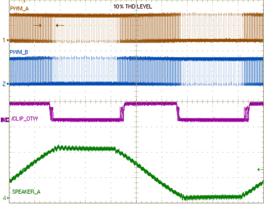
A built-in activity detector monitors the PWM activity of the OUT_X pins. TPA3223 is designed to drive unclipped output signals all the way to PVDD and GND rails. In case of audio signal clipping when applying excessive input signal voltage, or in case of CB3C current protection being active, the amplifier feedback loop of the audio channel will respond to this condition with a saturated state, and the output PWM signals will stop unless special circuitry is implemented to handle this situation. To prevent the output PWM signals from stopping in a clipping or CB3C situation, narrow pulses are injected to the gate drive to maintain output activity. The injected narrow pulses are injected at every 4th PWM frame, and thus the effective switching frequency during this state is reduced to 1/4 of the normal switching frequency.
Signal clipping is signaled on the OTW_CLIP pin and is self clearing when signal level reduces and the device reverts to normal operation. The OTW_CLIP pulses start at the onset to output clipping, typically at a THD level around 0.01%, resulting in narrow OTW_CLIP pulses starting with a pulse width of approximately 500 ns.
 Figure 9-15 Signal Clipping PWM and Speaker Output Signals