SLOS429C May 2004 – May 2016 TPA6204A1
PRODUCTION DATA.
- 1 Features
- 2 Applications
- 3 Description
- 4 Revision History
- 5 Device Comparison Table
- 6 Pin Configuration and Functions
- 7 Specifications
- 8 Parameter Measurement Information
- 9 Detailed Description
- 10Application and Implementation
- 11Power Supply Recommendations
- 12Layout
- 13Device and Documentation Support
- 14Mechanical, Packaging, and Orderable Information
パッケージ・オプション
デバイスごとのパッケージ図は、PDF版データシートをご参照ください。
メカニカル・データ(パッケージ|ピン)
- DRB|8
サーマルパッド・メカニカル・データ
- DRB|8
発注情報
7 Specifications
7.1 Absolute Maximum Ratings
over operating free-air temperature range (unless otherwise noted)(1)| MIN | MAX | UNIT | ||
|---|---|---|---|---|
| Supply voltage, VDD | –0.3 | 6 | V | |
| Input voltage, VI | –0.3 | VDD + 0.3 | V | |
| Continuous total power dissipation | See Dissipation Ratings | |||
| Operating free-air temperature, TA | –40 | 85 | °C | |
| Junction temperature, TJ | –40 | 150 | °C | |
| Storage temperature, Tstg | –65 | 150 | °C | |
(1) Stresses beyond those listed under Absolute Maximum Ratings may cause permanent damage to the device. These are stress ratings only, which do not imply functional operation of the device at these or any other conditions beyond those indicated under Recommended Operating Conditions. Exposure to absolute-maximum-rated conditions for extended periods may affect device reliability.
7.2 ESD Ratings
| VALUE | UNIT | |||
|---|---|---|---|---|
| V(ESD) | Electrostatic discharge | Human-body model (HBM), per ANSI/ESDA/JEDEC JS-001(1) | ±4000 | V |
| Charged-device model (CDM), per JEDEC specification JESD22-C101(2) | ±1500 | |||
(1) JEDEC document JEP155 states that 500-V HBM allows safe manufacturing with a standard ESD control process.
(2) JEDEC document JEP157 states that 250-V CDM allows safe manufacturing with a standard ESD control process.
7.3 Recommended Operating Conditions
over operating free-air temperature range (unless otherwise noted)| MIN | MAX | UNIT | ||
|---|---|---|---|---|
| Supply voltage, VDD | 2.5 | 5.5 | V | |
| High-level input voltage, VIH | SHUTDOWN | 1.55 | V | |
| Low-level input voltage, VIL | SHUTDOWN | 0.5 | V | |
| Operating free-air temperature, TA | –40 | 85 | °C | |
7.4 Thermal Information
| THERMAL METRIC(1) | TPA6204A1 | UNIT | |
|---|---|---|---|
| DRB (SON) | |||
| 8 PINS | |||
| RθJA | Junction-to-ambient thermal resistance | 50.3 | °C/W |
| RθJC(top) | Junction-to-case (top) thermal resistance | 69.2 | °C/W |
| RθJB | Junction-to-board thermal resistance | 25.5 | °C/W |
| ψJT | Junction-to-top characterization parameter | 1.8 | °C/W |
| ψJB | Junction-to-board characterization parameter | 25.6 | °C/W |
| RθJC(bot) | Junction-to-case (bottom) thermal resistance | 6.7 | °C/W |
(1) For more information about traditional and new thermal metrics, see the Semiconductor and IC Package Thermal Metrics application report, SPRA953.
7.5 Electrical Characteristics: TA = 25°C
over operating free-air temperature range (unless otherwise noted)| PARAMETER | TEST CONDITIONS | MIN | TYP | MAX | UNIT | ||
|---|---|---|---|---|---|---|---|
| VOS | Output offset voltage (measured differentially) | VI = 0 V differential, Gain = 1 V/V, VDD = 5.5 V | –9 | 0.3 | 9 | mV | |
| PSRR | Power supply rejection ratio | VDD = 2.5 V to 5.5 V | –85 | –60 | dB | ||
| VIC | Common mode input range | VDD = 2.5 V to 5.5 V | 0.5 | VDD – 0.8 | V | ||
| CMRR | Common mode rejection ratio | VDD = 5.5 V, VIC = 0.5 V to 4.7 V | –63 | –40 | dB | ||
| VDD = 2.5 V, VIC = 0.5 V to 1.7 V | –63 | –40 | |||||
| Low-output swing | RL = 8 Ω, VIN+ = VDD, Gain = 1 V/V, VIN− = 0 V or VIN+ = 0 V, VIN− = VDD |
VDD = 5.5 V | 0.45 | V | |||
| VDD = 3.6 V | 0.37 | ||||||
| VDD = 2.5 V | 0.26 | 0.4 | |||||
| High-output swing | RL = 8 Ω, VIN+ = VDD, Gain = 1 V/V, = 0 V or VIN− = VDD
VIN− VIN+ = 0 V |
VDD = 5.5 V | 4.95 | V | |||
| VDD = 3.6 V | 3.18 | ||||||
| VDD = 2.5 V | 2 | 2.13 | |||||
| | IIH | | High-level input current, SHUTDOWN | VDD = 5.5 V, VI = 5.8 V | 58 | 100 | µA | ||
| | IIL | | Low-level input current, SHUTDOWN | VDD = 5.5 V, VI = −0.3 V | 3 | 100 | µA | ||
| IQ | Quiescent current | VDD = 2.5 V to 5.5 V, no load | 4 | 6 | mA | ||
| I(SD) | Supply current | V(SHUTDOWN) ≤ 0.5 V, VDD = 2.5 V to 5.5 V, RL = 8 Ω |
0.01 | 1 | µA | ||
| Gain | RL = 8 Ω | 38 kΩ / RI | 40 kΩ / RI | 42 kΩ / RI | V/V | ||
| Resistance from shutdown to GND | 100 | kΩ | |||||
7.6 Operating Characteristics: TA = 25°C, Gain = 1 V/V
over operating free-air temperature range (unless otherwise noted)| PARAMETER | TEST CONDITIONS | MIN | TYP | MAX | UNIT | ||
|---|---|---|---|---|---|---|---|
| PO | Output power | THD + N = 1%, f = 1 kHz, RL = 8 Ω |
VDD = 5.5 V | 1.36 | W | ||
| VDD = 3.6 V | 0.72 | ||||||
| VDD = 2.5 V | 0.33 | ||||||
| THD + N = 10%, f = 1 kHz, RL = 8 Ω | VDD = 5.5 V | 1.7 | W | ||||
| VDD = 3.6 V | 0.85 | ||||||
| VDD = 2.5 V | 0.4 | ||||||
| THD+N | Total harmonic distortion + noise | VDD = 5 V, PO = 1 W, RL = 8 Ω, f = 1 kHz | 0.02% | ||||
| VDD = 3.6 V, PO = 0.5 W, RL = 8 Ω, f = 1 kHz | 0.02% | ||||||
| VDD = 2.5 V, PO = 200 mW, RL = 8 Ω, f = 1 kHz | 0.03% | ||||||
| kSVR | Supply ripple rejection ratio | VDD = 3.6 V, Inputs AC-grounded with Ci = 2 µF, V(RIPPLE) = 200 mVPP |
f = 217 Hz | –80 | dB | ||
| f = 20 Hz to 20 kHz | –70 | ||||||
| SNR | Signal-to-noise ratio | VDD = 5 V, PO = 1 W, RL = 8 Ω | 105 | dB | |||
| Vn | Output voltage noise | VDD = 3.6 V, f = 20 Hz to 20 kHz, Inputs AC-grounded with Ci = 2 μF | No weighting | 15 | µVRMS | ||
| A weighting | 12 | ||||||
| CMRR | Common-mode rejection ratio | VDD = 3.6 V VIC = 1 VPP | f = 217 Hz | –65 | dB | ||
| RF | Feedback resistance | 38 | 40 | 44 | kΩ | ||
| Start-up time from shutdown | VDD = 3.6 V, CBYPASS = 0.1 μF | 27 | ms | ||||
7.7 Dissipation Ratings
| PACKAGE | TA ≤ 25°C POWER RATINGS | DERATING FACTOR | TA = 70°C POWER RATINGS | TA = 85°C POWER RATINGS |
|---|---|---|---|---|
| DRB | 2.7 W | 21.8 mW/°C | 1.7 W | 1.4 W |
7.8 Typical Characteristics
Table 1. Table of Graphs
| FIGURE | |||
|---|---|---|---|
| PO | Output power | vs Supply voltage | Figure 1 |
| vs Load resistance | Figure 2 | ||
| PD | Power dissipation | vs Output power | Figure 3 |
| THD+N | Total harmonic distortion + noise | vs Output power | Figure 4 |
| vs Frequency | Figure 5 | ||
| vs Common-mode input voltage | Figure 6 | ||
| KSVR | Supply voltage rejection ratio | vs Frequency | Figure 7 |
| GSM Power supply rejection | vs Time | Figure 8 | |
| GSM Power supply rejection | vs Frequency | Figure 9 | |
| Closed-loop gain/phase | vs Frequency | Figure 10 | |
| Open-loop gain/phase | vs Frequency | Figure 11 | |
| IDD | Supply current | vs Supply voltage | Figure 12 |
| vs Shutdown voltage | Figure 13 | ||
| Start-up time | vs Bypass capacitor | Figure 14 | |
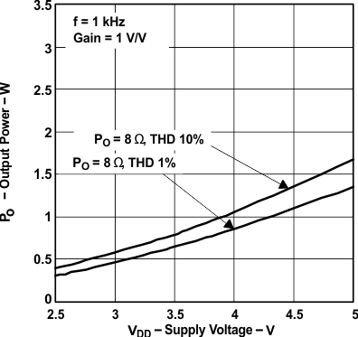 Figure 1. Output Power vs Supply Voltage
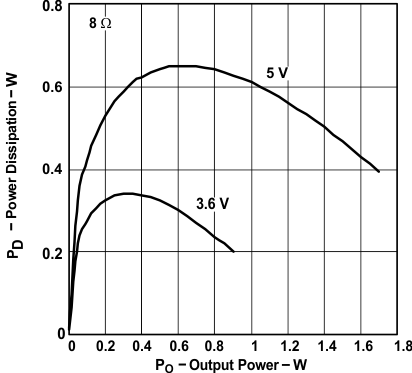 Figure 3. Power Dissipation vs Output Power
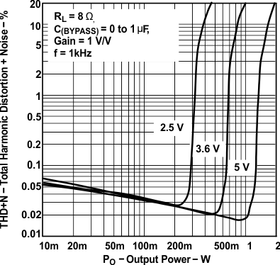 Figure 5. Total Harmonic Distortion + Noise vs Output Power
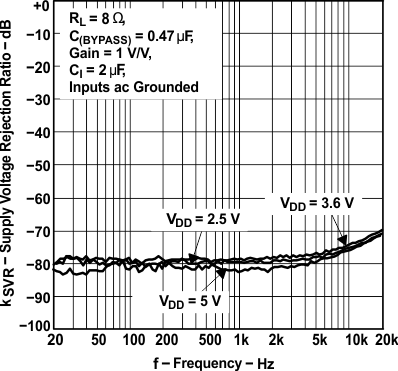 Figure 7. Supply Voltage Rejection Ratio vs Frequency
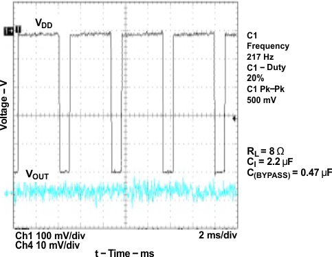 Figure 9. GSM Power Supply Rejection vs Time
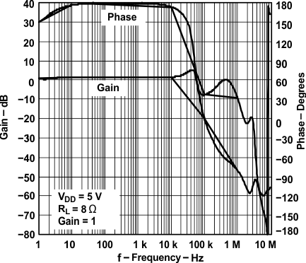 Figure 11. Closed-Loop Gain/Phase vs Frequency
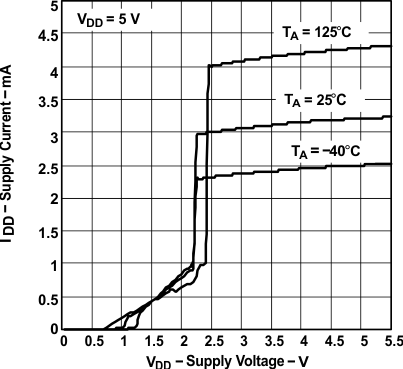 Figure 13. Supply Current vs Supply Voltage
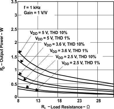 Figure 2. Output Power vs Load Resistance
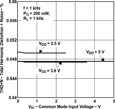 Figure 4. Total Harmonic Distortion + Noise vs Common-Mode Input Voltage
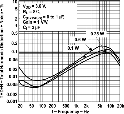 Figure 6. Total Harmonic Distortion + Noise vs Frequency
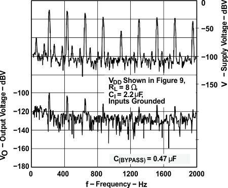 Figure 8. GSM Power Supply Rejection vs Frequency
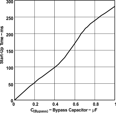 Figure 10. Start-Up Time vs Bypass Capacitor
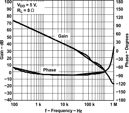 Figure 12. Open-Loop Gain/Phase vs Frequency
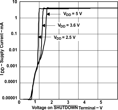 Figure 14. Supply Current vs Supply Voltage