SLVSDG4B March 2016 – August 2016 TPD1E04U04
PRODUCTION DATA.
- 1 Features
- 2 Applications
- 3 Description
- 4 Revision History
- 5 Pin Configuration and Functions
- 6 Specifications
-
7 Detailed Description
- 7.1 Overview
- 7.2 Functional Block Diagram
- 7.3
Feature Description
- 7.3.1 IEC 61000-4-2 ESD Protection
- 7.3.2 IEC 61000-4-4 EFT Protection
- 7.3.3 IEC 61000-4-5 Surge Protection
- 7.3.4 IO Capacitance
- 7.3.5 Ultra-Low ESD Clamping Voltage
- 7.3.6 Low RDYN
- 7.3.7 DC Breakdown Voltage
- 7.3.8 Ultra Low Leakage Current
- 7.3.9 Supports High Speed Interfaces
- 7.3.10 Industrial Temperature Range
- 7.3.11 Easy Flow-Through Routing Package
- 7.4 Device Functional Modes
- 8 Application and Implementation
- 9 Power Supply Recommendations
- 10Layout
- 11Device and Documentation Support
- 12Mechanical, Packaging, and Orderable Information
パッケージ・オプション
デバイスごとのパッケージ図は、PDF版データシートをご参照ください。
メカニカル・データ(パッケージ|ピン)
- DPY|2
- DPL|2
サーマルパッド・メカニカル・データ
- DPL|2
発注情報
8 Application and Implementation
NOTE
Information in the following applications sections is not part of the TI component specification, and TI does not warrant its accuracy or completeness. TI’s customers are responsible for determining suitability of components for their purposes. Customers should validate and test their design implementation to confirm system functionality.
8.1 Application Information
The TPD1E04U04 is a diode type TVS which is used to provide a path to ground for dissipating ESD events on high-speed signal lines between a human interface connector and a system. As the current from ESD passes through the TVS, only a small voltage drop is present across the diode. This is the voltage presented to the protected IC. The low RDYN of the triggered TVS holds this voltage, VCLAMP, to a safe level for the protected IC.
8.2 Typical Application
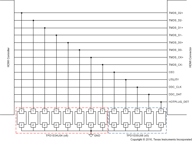
 Figure 13. HDMI 2.0 ESD Schematic
8.2.1 Design Requirements
For this design example eight TPD1E04U04 devices and five TPD1E05U06 devices are being used in a HDMI 2.0 application. This provides a complete ESD protection scheme.
Given the HDMI 2.0 application, the parameters listed in Table 1 are known.
Table 1. Design Parameters
| DESIGN PARAMETER | VALUE |
|---|---|
| Signal range on TMDS lines | 0 V to 3.6 V |
| Operating frequency on TMDS lines | up to 3 GHz |
| Signal range on control lines | 0 V to 5.5 V |
8.2.2 Detailed Design Procedure
8.2.2.1 Signal Range
The TPD1E04U04 supports signal ranges between 0 V and 3.6 V, which supports the TMDS pairs on the HDMI 2.0 application. The TPD1E05U06 supports signal ranges between 0 V and 5.5 V, which supports the control lines.
8.2.2.2 Operating Frequency
The TPD1E04U04 has a 0.5-pF (typical) capacitance, which supports the HDMI 2.0 data rates of 6-Gbps. The TPD1E05U06 has a 0.5-pF (typical) capacitance as well, which easily supports the control line data rates.
8.2.3 Application Curves


(With TPD1E04U04)