JAJSJE7C March 2016 – August 2020 TPD3S014-Q1
PRODUCTION DATA
- 1 特長
- 2 アプリケーション
- 3 概要
- 4 Revision History
- 5 Pin Configuration and Functions
-
6 Specifications
- 6.1 Absolute Maximum Ratings
- 6.2 ESD Ratings—AEC Specification
- 6.3 ESD Ratings—IEC Specification
- 6.4 ESD Ratings—ISO Specification
- 6.5 Recommended Operating Conditions
- 6.6 Thermal Information
- 6.7 Electrical Characteristics: TJ = TA = 25°C
- 6.8 Electrical Characteristics: –40°C ≤ TA ≤ 105°C
- 6.9 Typical Characteristics
- 7 Parameter Measurement Information
- 8 Detailed Description
- 9 Application and Implementation
- 10Power Supply Recommendations
- 11Layout
- 12Device and Documentation Support
- 13Mechanical, Packaging, and Orderable Information
11.3 Power Dissipation and Junction Temperature
anged Temperature from 125°C to 105°C in Power Dissipation and Junction Temperature section
anged Temperature from 125°C to 105°C in Power Dissipation and Junction Temperature section
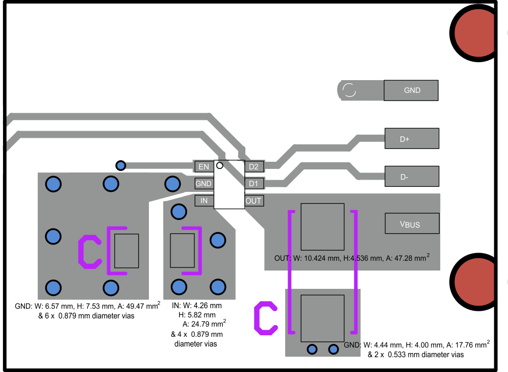
It is good design practice to estimate power dissipation and maximum expected junction temperature of the TPD3S014-Q1. The system designer can control choices of the devices proximity to other power dissipating devices and printed circuit board (PCB) design based on these calculations. These have a direct influence on maximum junction temperature. Other factors, such as airflow and maximum ambient temperature, are often determined by system considerations. It is important to remember that these calculations do not include the effects of adjacent heat sources, and enhanced or restricted air flow. Addition of extra PCB copper area around these devices is recommended to reduce the thermal impedance and maintain the junction temperature as low as practical. In particular, connect the GND pin to a large ground plane for the best thermal dissipation. The following PCB layout example in Figure 11-2 was used to determine the RθJA Custom thermal impedances noted in the Thermal Information table. It is based on the use of the JEDEC high-k circuit board construction with 4, 1 oz. copper weight layers (2 signal and 2 plane).
 Figure 11-2 PCB Layout Example
The following procedure requires iteration a power loss is because of the internal MOSFET I2 × RDS(ON), and RDS(ON) is a function of the junction temperature. See Equation 1. As an initial estimate, use the RDS(ON) at 105°C from the Typical Characteristics, and the preferred package thermal resistance for the preferred board construction from the Thermal Information table.
where
- IOUT = Rated OUT pin current (A)
- RDS(ON) = Power switch on-resistance at an assumed TJ (Ω)
- TA = Maximum ambient temperature (°C)
- TJ = Maximum junction temperature (°C)
- RθJA = Thermal resistance (°C/W)
If the calculated TJ is substantially different from the original assumption, estimate a new value of RDS(ON) using the typical characteristic plot and recalculate.
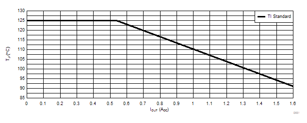
If the resulting TJ is not less than 125°C, try a PCB construction with a lower RθJA. The junction temperature derating curve based on the TI standard reliability duration is shown in Figure 11-3.
 Figure 11-3 Junction Temperature Derating Curve