JAJSJE7C March 2016 – August 2020 TPD3S014-Q1
PRODUCTION DATA
- 1 特長
- 2 アプリケーション
- 3 概要
- 4 Revision History
- 5 Pin Configuration and Functions
-
6 Specifications
- 6.1 Absolute Maximum Ratings
- 6.2 ESD Ratings—AEC Specification
- 6.3 ESD Ratings—IEC Specification
- 6.4 ESD Ratings—ISO Specification
- 6.5 Recommended Operating Conditions
- 6.6 Thermal Information
- 6.7 Electrical Characteristics: TJ = TA = 25°C
- 6.8 Electrical Characteristics: –40°C ≤ TA ≤ 105°C
- 6.9 Typical Characteristics
- 7 Parameter Measurement Information
- 8 Detailed Description
- 9 Application and Implementation
- 10Power Supply Recommendations
- 11Layout
- 12Device and Documentation Support
- 13Mechanical, Packaging, and Orderable Information
8.3.2 Enable
The logic enable input (EN) controls the power switch, bias for the charge pump, driver, and other circuits. The supply current is reduced to less than 1 µA when the TPD3S014-Q1 is disabled. The enable input is compatible with both TTL and CMOS logic levels.
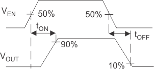
The turnon and turnoff times (tON, tOFF) are composed of a delay and a rise or fall time (tR, tF). The delay times are internally controlled. The rise time is controlled by both the TPD3S014-Q1 and the external loading (especially capacitance). The TPD3S014-Q1 fall time is controlled by the loading (R and C), and the output discharge (RPD). An output load consisting of only a resistor experiences a fall time set by the TPD3S014-Q1. An output load with parallel R and C elements experiences a fall time determined by the (R × C) time constant if it is longer than the TPD3S014-Q1 tF. See Figure 8-1 and Figure 8-2 showing tR, tF, tON, and tOFF. The enable must not be left open; it may be tied to VIN.
 Figure 8-1 Power-On and Power-Off Timing
 Figure 8-2 Enable Timing, Active-High Enable