JAJSJN8C January   2016  – August 2020 TPD3S714-Q1

PRODUCTION DATA  

  1. 特長
  2. アプリケーション
  3. 概要
  4. Revision History
  5. Pin Configuration and Functions
    1.     Pin Functions
  6. Specifications
    1. 6.1 Absolute Maximum Ratings
    2. 6.2 ESD Ratings—AEC Specification
    3. 6.3 ESD Ratings—IEC Specification
    4. 6.4 ESD Ratings—ISO Specification
    5. 6.5 Recommended Operating Conditions
    6. 6.6 Thermal Information
    7. 6.7 Electrical Characteristics
    8. 6.8 Timing Requirements
    9. 6.9 Typical Characteristics
  7. Parameter Measurement Information
  8. Detailed Description
    1. 8.1 Overview
    2. 8.2 Functional Block Diagram
    3. 8.3 Feature Description
      1. 8.3.1  AEC-Q100 Qualified
      2. 8.3.2  Short-to-Battery and Short-to-Ground Protection on VBUS_CON
      3. 8.3.3  Short-to-Battery and Short-to-VBUS Protection on VD+, VD–
      4. 8.3.4  ESD Protection on VBUS_CON, VD+, VD–
      5. 8.3.5  Low RON nFET VBUS Switch
      6. 8.3.6  High Speed Data Switches
      7. 8.3.7  Hiccup Current Limit
      8. 8.3.8  Fast Overvoltage Response Time
      9. 8.3.9  Integrated Input Enable
      10. 8.3.10 Fault Output Signal
      11. 8.3.11 Thermal Shutdown Feature
      12. 8.3.12 16-pin SSOP Package
    4. 8.4 Device Functional Modes
      1. 8.4.1 Normal Operation
      2. 8.4.2 Overvoltage Condition
      3. 8.4.3 Overcurrent Condition
      4. 8.4.4 Short-Circuit Condition
      5. 8.4.5 Device Logic Tables
  9. Application and Implementation
    1. 9.1 Application Information
    2. 9.2 Typical Application
      1. 9.2.1 Design Requirements
      2. 9.2.2 Detailed Design Procedure
        1. 9.2.2.1 Short-to-Battery Tolerance
        2. 9.2.2.2 Maximum Current on VBUS
        3. 9.2.2.3 USB Data Rate
      3. 9.2.3 Application Curves
  10. 10Power Supply Recommendations
    1. 10.1 VBUS Path
    2. 10.2 VIN Pin
  11. 11Layout
    1. 11.1 Layout Guidelines
    2. 11.2 Layout Example
  12. 12Device and Documentation Support
    1. 12.1 Documentation Support
      1. 12.1.1 Related Documentation
    2. 12.2 Receiving Notification of Documentation Updates
    3. 12.3 Support Resources
    4. 12.4 Trademarks
    5. 12.5 Electrostatic Discharge Caution
    6. 12.6 Glossary
  13. 13Mechanical, Packaging, and Orderable Information

パッケージ・オプション

メカニカル・データ(パッケージ|ピン)
サーマルパッド・メカニカル・データ
発注情報

Mechanical, Packaging, and Orderable Information

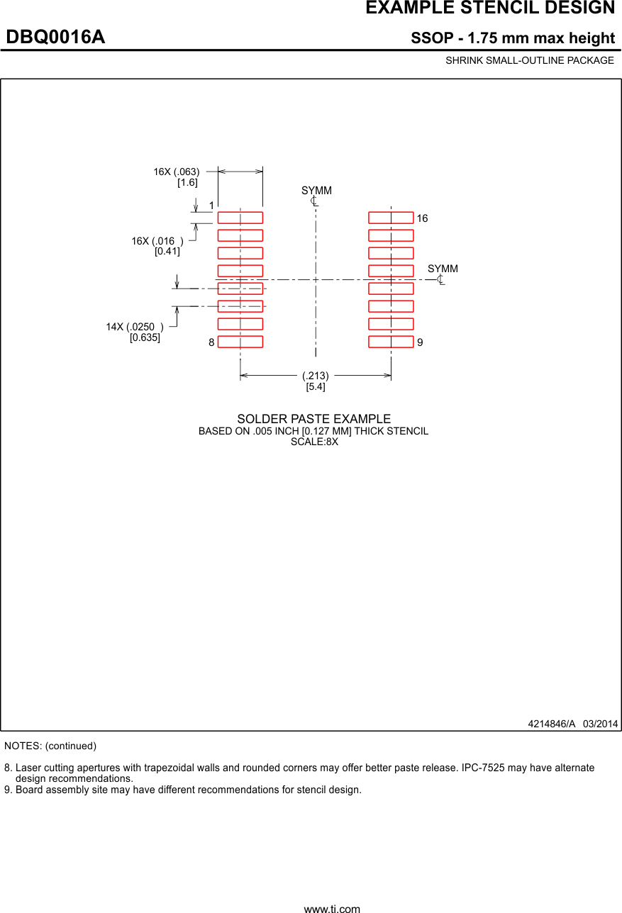
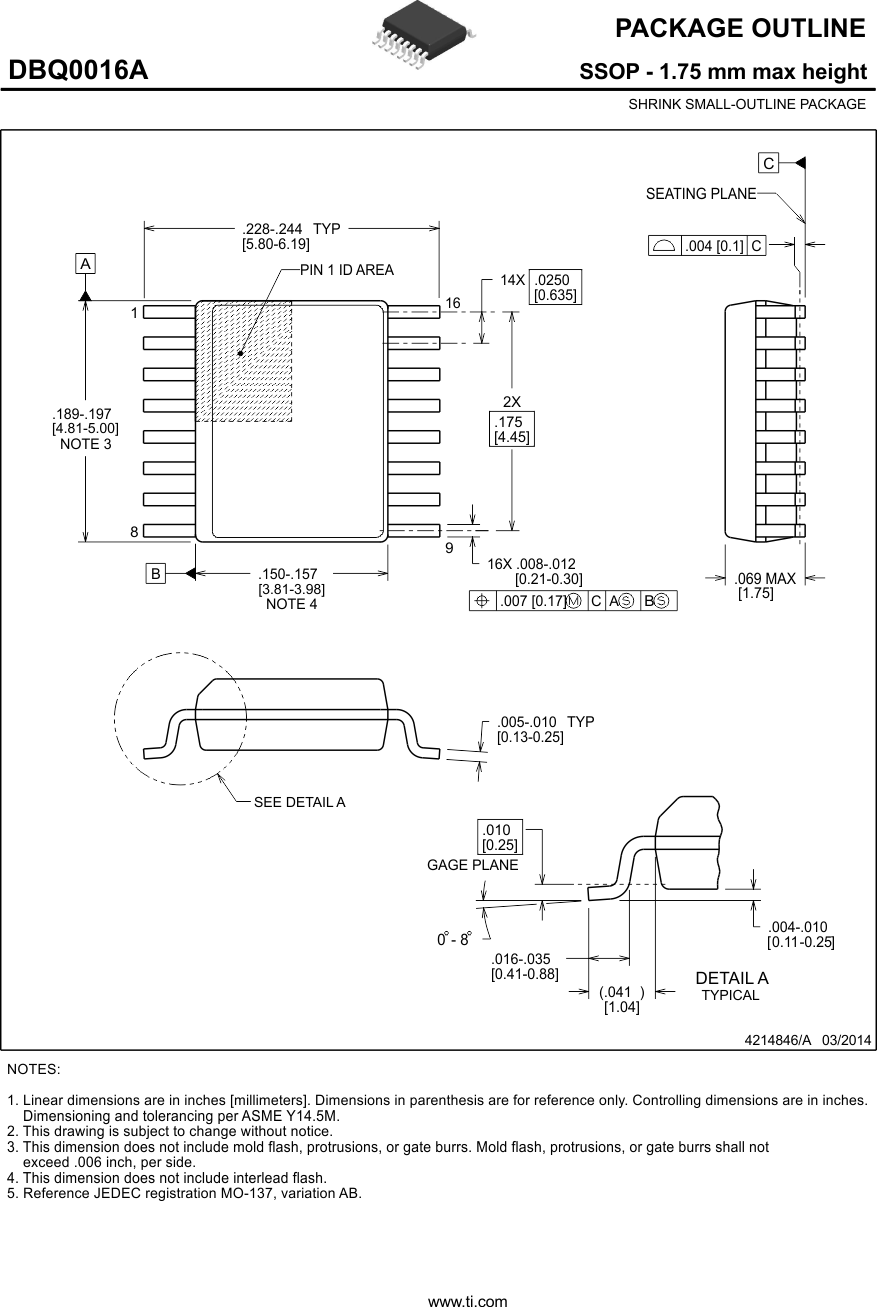
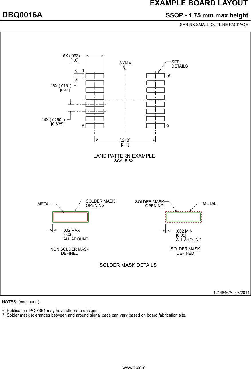
The following pages include mechanical, packaging, and orderable information. This information is the most current data available for the designated devices. This data is subject to change without notice and revision of this document. For browser-based versions of this data sheet, refer to the left-hand navigation.
GUID-8A2B1D47-046A-44B1-AA90-CB97DC815739-low.gif
GUID-864E6DFB-E51B-49EF-A133-AF496EB4D1CC-low.gif
GUID-E1DCE304-2570-490B-9820-E4CE7DF29C6F-low.gif