JAJSDV1A June 2017 – September 2017 TPD4E02B04-Q1
PRODUCTION DATA.
- 1 特長
- 2 アプリケーション
- 3 概要
- 4 改訂履歴
- 5 Pin Configuration and Functions
- 6 Specifications
-
7 Detailed Description
- 7.1 Overview
- 7.2 Functional Block Diagram
- 7.3
Feature Description
- 7.3.1 AEC-Q101 Qualified
- 7.3.2 ISO 10605 ESD Protection
- 7.3.3 IEC 61000-4-2 ESD Protection
- 7.3.4 IEC 61000-4-4 EFT Protection
- 7.3.5 IEC 61000-4-5 Surge Protection
- 7.3.6 IO Capacitance
- 7.3.7 DC Breakdown Voltage
- 7.3.8 Ultra Low Leakage Current
- 7.3.9 Low ESD Clamping Voltage
- 7.3.10 Supports High Speed Interfaces
- 7.3.11 Industrial Temperature Range
- 7.3.12 Easy Flow-Through Routing Package
- 7.4 Device Functional Modes
- 8 Application and Implementation
- 9 Power Supply Recommendations
- 10Layout
- 11デバイスおよびドキュメントのサポート
- 12メカニカル、パッケージ、および注文情報
パッケージ・オプション
メカニカル・データ(パッケージ|ピン)
- DQA|10
サーマルパッド・メカニカル・データ
- DQA|10
発注情報
7 Detailed Description
7.1 Overview
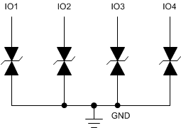
The TPD4E02B04-Q1 is an automotive-qualified bidirectional ESD Protection Diode with ultra-low capacitance. This device can dissipate ESD strikes above the maximum level specified by the IEC 61000-4-2 (Level 4) International Standard. The ultra-low capacitance makes this device ideal for protecting any super high-speed signal pins.
7.2 Functional Block Diagram

7.3 Feature Description
7.3.1 AEC-Q101 Qualified
This device is qualified to AEC-Q101 standards and is qualified to operate from –40°C to +125°C.
7.3.2 ISO 10605 ESD Protection
The I/O pins can withstand ESD events of at least ±10-kV contact and ±10-kV air gap according to the ISO 10605 (330 pF, 330 Ω) standard. The device diverts the current to ground.
7.3.3 IEC 61000-4-2 ESD Protection
The I/O pins can withstand ESD events up to ±12-kV contact and ±15-kV air gap. An ESD-surge clamp diverts the current to ground.
7.3.4 IEC 61000-4-4 EFT Protection
The I/O pins can withstand an electrical fast transient burst of up to 80 A (5/50 ns waveform, 4 kV with 50-Ω impedance). An ESD-surge clamp diverts the current to ground.
7.3.5 IEC 61000-4-5 Surge Protection
The I/O pins can withstand surge events up to 2 A and 17 W (8/20 µs waveform). An ESD-surge clamp diverts this current to ground.
7.3.6 IO Capacitance
The capacitance between each I/O pin to ground is 0.25 pF (typical). This device supports data rates up to 10 Gbps.
7.3.7 DC Breakdown Voltage
The DC breakdown voltage of each I/O pin is a minimum of ±5.5 V. This ensures that sensitive equipment is protected from surges above the reverse standoff voltage of ±3.6 V.
7.3.8 Ultra Low Leakage Current
The I/O pins feature an ultra-low leakage current of 10 nA (maximum) with a bias of ±2.5 V.
7.3.9 Low ESD Clamping Voltage
The I/O pins feature an ESD clamp that is capable of clamping the voltage to 8.8 V (IPP = 5 A).
7.3.10 Supports High Speed Interfaces
This device is capable of supporting high speed interfaces up to 10 Gbps, because of the extremely low IO capacitance.
7.3.11 Industrial Temperature Range
This device features an industrial operating range of –40°C to +125°C.
7.3.12 Easy Flow-Through Routing Package
The layout of this device makes it simple and easy to add protection to an existing layout. The packages offers flow-through routing, requiring minimal modification to an existing layout.
7.4 Device Functional Modes
The TPD4E02B04-Q1 is a passive integrated circuit that triggers when voltages are above VBRF or below VBRR. During ESD events, voltages as high as ±15 kV (air) can be directed to ground via the internal diode network. When the voltages on the protected line fall below the trigger levels of the TPD4E02B04-Q1 (usually within 10s of nano-seconds) the device reverts to passive.