JAJSFN1 June 2018 TPD6S300A
PRODUCTION DATA.
- 1 特長
- 2 アプリケーション
- 3 概要
- 4 改訂履歴
- 5 概要(続き)
- 6 Device Comparison Table
- 7 Pin Configuration and Functions
- 8 Specifications
-
9 Detailed Description
- 9.1 Overview
- 9.2 Functional Block Diagram
- 9.3
Feature Description
- 9.3.1 4-Channels of Short-to-VBUS Overvoltage Protection (CC1, CC2, SBU1, SBU2 Pins or CC1, CC2, DP, DM Pins): 24-VDC Tolerant
- 9.3.2 6-Channels of IEC 61000-4-2 ESD Protection (CC1, CC2, SBU1, SBU2, DP, DM Pins)
- 9.3.3 CC1, CC2 Overvoltage Protection FETs 600 mA Capable for Passing VCONN Power
- 9.3.4 CC Dead Battery Resistors Integrated for Handling the Dead Battery Use Case in Mobile Devices
- 9.3.5 Advantages over TPD6S300
- 9.3.6 3-mm × 3-mm WQFN Package
- 9.4 Device Functional Modes
- 10Application and Implementation
- 11Power Supply Recommendations
- 12Layout
- 13デバイスおよびドキュメントのサポート
- 14メカニカル、パッケージ、および注文情報
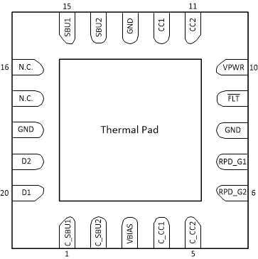
7 Pin Configuration and Functions
RUK Package
20-Pin WQFN
Top View

Pin Functions
| PIN | TYPE(1) | DESCRIPTION | |
|---|---|---|---|
| NO. | NAME | ||
| 1 | C_SBU1 | I/O | Connector side of the SBU1 OVP FET. Connect to either SBU pin of the USB Type-C connector. Alternatively, connect to either USB2.0 pin of the USB Type-C connector to protect the USB2.0 pins instead of the SBU pins |
| 2 | C_SBU2 | I/O | Connector side of the SBU2 OVP FET. Connect to either SBU pin of the USB Type-C connector. Alternatively, connect to either USB2.0 pin of the USB Type-C connector to protect the USB2.0 pins instead of the SBU pins |
| 3 | VBIAS | P | Pin for ESD support capacitor. Place a 0.1-µF capacitor on this pin to ground |
| 4 | C_CC1 | I/O | Connector side of the CC1 OVP FET. Connect to either CC pin of the USB Type-C connector |
| 5 | C_CC2 | I/O | Connector side of the CC2 OVP FET. Connect to either CC pin of the USB Type-C connector |
| 6 | RPD_G2 | I/O | Short to C_CC2 if dead battery resistors are needed. If dead battery resistors are not needed, short pin to GND |
| 7 | RPD_G1 | I/O | Short to C_CC1 if dead battery resistors are needed. If dead battery resistors are not needed, short pin to GND |
| 8 | GND | GND | Ground |
| 9 | FLT | O | Open drain for fault reporting |
| 10 | VPWR | P | 2.7-V to 4.5-V power supply |
| 11 | CC2 | I/O | System side of the CC2 OVP FET. Connect to either CC pin of the CC/PD controller |
| 12 | CC1 | I/O | System side of the CC1 OVP FET. Connect to either CC pin of the CC/PD controller |
| 13 | GND | GND | Ground |
| 14 | SBU2 | I/O | System side of the SBU2 OVP FET. Connect to either SBU pin of the SBU MUX. Alternatively, connect to either USB2.0 pin of the USB2.0 Phy when protecting the USB2.0 pins instead of protecting the SBU pins |
| 15 | SBU1 | I/O | System side of the SBU1 OVP FET. Connect to either SBU pin of the SBU MUX. Alternatively, connect to either USB2.0 pin of the USB2.0 Phy when protecting the USB2.0 pins instead of protecting the SBU pins |
| 16 | N.C. | I/O | Unused pin. Connect to Ground |
| 17 | N.C. | I/O | Unused pin. Connect to Ground |
| 18 | GND | GND | Ground |
| 19 | D2 | I/O | USB2.0 IEC ESD protection. Connect to any of the USB2.0 pins of the USB Type-C connector |
| 20 | D1 | I/O | USB2.0 IEC ESD protection. Connect to any of the USB2.0 pins of the USB Type-C connector |
| — | Thermal Pad | GND | Internally connected to GND. Used as a heatsink. Connect to the PCB GND plane |
(1) I = input, O = output, I/O = input and output, GND = ground, P = power