JAJSO48E October   2004  – May 2022 TPIC1021

PRODUCTION DATA  

  1. 特長
  2. アプリケーション
  3. 概要
  4. Revision History
  5. 概要 (続き)
  6. Pin Configuration and Functions
  7. Specifications
    1. 7.1 Absolute Maximum Ratings
    2. 7.2 ESD Ratings
    3. 7.3 Recommended Operating Conditions
    4. 7.4 Thermal Information
    5. 7.5 Electrical Characteristics
    6. 7.6 Timing Requirements
    7. 7.7 Typical Characteristics
  8. Detailed Description
    1. 8.1 Overview
    2. 8.2 Functional Block Diagram
    3. 8.3 Feature Description
      1. 8.3.1 LIN Bus Pin
        1. 8.3.1.1 Transmitter Characteristics
        2. 8.3.1.2 Receiver Characteristics
      2. 8.3.2 Transmit Input Pin (TXD)
        1. 8.3.2.1 TXD Dominant State Timeout
      3. 8.3.3 Receive Output Pin (RXD)
        1. 8.3.3.1 RXD Wake-up Request
      4. 8.3.4 Ground (GND)
      5. 8.3.5 Enable Input Pin (EN)
      6. 8.3.6 NWake Input Pin (NWake)
      7. 8.3.7 Inhibit Output Pin (INH)
    4. 8.4 Device Functional Modes
      1. 8.4.1 Operating States
        1. 8.4.1.1 Normal Mode
        2. 8.4.1.2 Low Power Mode
        3. 8.4.1.3 Wake-Up Events
        4. 8.4.1.4 Standby Mode
      2. 8.4.2 Supply Voltage (VSUP)
  9. Application and Implementation
    1. 9.1 Application Information
    2. 9.2 Typical Application
      1. 9.2.1 Design Requirements
      2. 9.2.2 Detailed Design Procedure
      3. 9.2.3 Application Curves
    3. 9.3 Power Supply Recommendations
    4. 9.4 Layout
      1. 9.4.1 Layout Guidelines
      2. 9.4.2 Layout Example
  10. 10Device and Documentation Support
    1. 10.1 Receiving Notification of Documentation Updates
    2. 10.2 サポート・リソース
    3. 10.3 Trademarks
    4. 10.4 Electrostatic Discharge Caution
    5. 10.5 Glossary
  11. 11Mechanical, Packaging, and Orderable Information

パッケージ・オプション

デバイスごとのパッケージ図は、PDF版データシートをご参照ください。

メカニカル・データ(パッケージ|ピン)
  • D|8
サーマルパッド・メカニカル・データ
発注情報

Standby Mode

This mode is entered whenever a wake-up event occurs via the LIN bus or NWake pin while the TPIC1021 is in low power mode. The LIN bus responder termination circuit and the INH pin are turned on when standby mode is entered. The application system powers up once the INH pin is driven high assuming it is using a voltage regulator connected via INH pin. Standby Mode is signaled via a low level on RXD pin.

When EN pin is set high while the TPIC1021 is in Standby Mode the device returns to Normal Mode and the normal transmission paths from TXD to LIN bus and LIN bus to RXD are turned on.
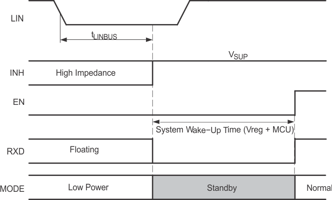
GUID-DC1BC198-4FD1-415C-9813-58AD51BC06E8-low.gifFigure 8-2 Wake-Up Via LIN Bus Timing Diagram
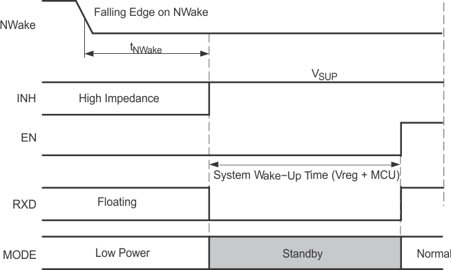
GUID-17A91F99-43E2-436F-AB5B-422286B6B42B-low.gifFigure 8-3 Wake-Up Via NWake Timing Diagram