JAJSG91B June 2015 – September 2018 TPL5111
PRODUCTION DATA.
- 1 特長
- 2 アプリケーション
- 3 概要
- 4 改訂履歴
- 5 Pin Configuration and Functions
- 6 Specifications
- 7 Detailed Description
- 8 Application and Implementation
- 9 Power Supply Recommendations
- 10Layout
- 11デバイスおよびドキュメントのサポート
- 12メカニカル、パッケージ、および注文情報
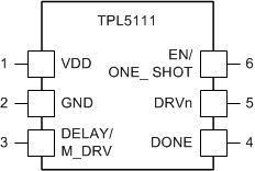
5 Pin Configuration and Functions
DDC Package
6-Lead SOT-23
Top View

Pin Functions
| PIN | TYPE(1) | DESCRIPTION | APPLICATION INFORMATION | |
|---|---|---|---|---|
| NO. | NAME | |||
| 1 | VDD | P | Supply voltage | |
| 2 | GND | G | Ground | |
| 3 | DELAY/ M_DRV | I | Time interval configuration (during power on) and logic input for manual Power ON | Resistance between this pin and GND is used to select the time interval. The manual Power ON signal (logic HIGH) can also connected to this pin. |
| 4 | DONE | I | Logic Input for watchdog functionality | Digital signal driven by the µC to indicate successful processing. |
| 5 | DRVn | O | Power Gating output signal generated every tIP | The ENABLE pin of the LDO or DC-DC converter is connected to this pin. DRVn is active HIGH. |
| 6 | EN/ ONE_SHOT | I | Select mode of operation | When EN/ONE_SHOT = HIGH, the TPL5111 works as a TIMER. When EN/ONE_SHOT = LOW, the TPL5111 asserts DRVn one time for the programmed time interval. In this mode, the DRVn signal may be manually asserted by applying a logic HIGH to the DELAY/M_DRV pin. |
(1) G= Ground, P= Power, O= Output, I= Input.