JAJSGO4D November 2018 – December 2019 TPS1HA08-Q1
PRODUCTION DATA.
- 1 特長
- 2 アプリケーション
- 3 概要
- 4 改訂履歴
- 5 Device Comparison Table
- 6 Pin Configuration and Functions
- 7 Specifications
- 8 Parameter Measurement Information
-
9 Detailed Description
- 9.1 Overview
- 9.2 Functional Block Diagram
- 9.3
Feature Description
- 9.3.1 Protection Mechanisms
- 9.3.2 Diagnostic Mechanisms
- 9.3.3 Enable Watchdog
- 9.4 Device Functional Modes
- 10Application and Implementation
- 11Power Supply Recommendations
- 12Layout
- 13デバイスおよびドキュメントのサポート
- 14メカニカル、パッケージ、および注文情報
パッケージ・オプション
メカニカル・データ(パッケージ|ピン)
- PWP|16
サーマルパッド・メカニカル・データ
- PWP|16
発注情報
7.7 SNS Timing Characteristics
VBB = 8 to 18 V, TJ = –40°C to 150°C (unless otherwise noted)| PARAMETER | TEST CONDITIONS | MIN | TYP | MAX | UNIT | |
|---|---|---|---|---|---|---|
| SNS TIMING - CURRENT SENSE | ||||||
| tSNSION1 | Settling time from rising edge of DIA_EN | VEN = 5 V, VDIA_EN = 0 V to 5 V
RSNS = 1 kΩ, RL = 2.6 Ω |
40 | µs | ||
| tSNSION2 | Settling time from rising edge of EN | VEN = VDIA_EN = 0 V to 5 V
RSNS = 1 kΩ, RL = 2.6 Ω |
180 | µs | ||
| tSNSION3 | Settling time from rising edge of EN | VEN = 0 V to 5 V, VDIA_EN = 5 V
RSNS = 1 kΩ, RL = 2.6 Ω |
180 | µs | ||
| tSNSIOFF1 | Settling time from falling edge of DIA_EN | VEN = 5 V, VDIA_EN = 5 V to 0 V
RSNS = 1 kΩ, RL = 2.6 Ω |
20 | µs | ||
| tSETTLEH | Settling time from rising edge of load step | VEN = 5 V, VDIA_EN = 5 V
RSNS = 1 kΩ, IOUT = 1 A to 5 A |
20 | µs | ||
| tSETTLEL | Settling time from falling edge of load step | VEN = 5 V, VDIA_EN = 5 V
RSNS = 1 kΩ, IOUT = 5 A to 1 A |
20 | µs | ||
| SNS TIMING - TEMPERATURE SENSE | ||||||
| tSNSTON1 | Settling time from rising edge of DIA_EN | VEN = 5 V, VDIA_EN = 0 V to 5 V
RSNS = 1 kΩ |
40 | µs | ||
| tSNSTON2 | Settling time from rising edge of DIA_EN | VEN = 0 V, VDIA_EN = 0 V to 5 V
RSNS = 1 kΩ |
70 | µs | ||
| tSNSTOFF | Settling time from falling edge of DIA_EN | VEN = X, VDIA_EN = 5 V to 0 V
RSNS = 1 kΩ |
20 | µs | ||
| SNS TIMING - VOLTAGE SENSE | ||||||
| tSNSVON1 | Settling time from rising edge of DIA_EN | VEN = 5 V, VDIA_EN = 0 V to 5 V
RSNS = 1 kΩ |
40 | µs | ||
| tSNSVON2 | Settling time from rising edge of DIA_EN | VEN = 0 V, VDIA_EN = 0 V to 5 V
RSNS = 1 kΩ |
70 | µs | ||
| tSNSVOFF | Settling time from falling edge of DIA_EN | VEN = X, VDIA_EN = 5 V to 0 V
RSNS = 1 kΩ |
20 | µs | ||
| SNS TIMING - MULTIPLEXER | ||||||
| tMUX | Settling time from temperature sense to current sense | VEN= X, VDIA_EN = 5 V
VSEL1 = 5 V to 0 V, VSEL2 = 0 V RSNS = 1 kΩ, RL = 2.6 Ω |
60 | µs | ||
| Settling time from temperature sense to voltage sense | VEN = X, VDIA_EN = 5 V
VSEL1 = 5 V, VSEL2 = 0 V to 5 V RSNS = 1 kΩ |
60 | µs | |||
| Settling time from voltage sense to temperature sense | VEN = X, VDIA_EN = 5 V
VSEL1 = 5 V, VSEL2 = 5 V to 0 V RSNS = 1 kΩ |
60 | µs | |||
| Settling time from voltage sense to current sense | VEN = X, VDIA_EN = 5 V
VSEL1 = VSEL2 = 5 V to 0 V, RSNS = 1 kΩ, RL = 2.6 Ω |
60 | µs | |||
| Settling time from current sense to temperature sense | VEN = X, VDIA_EN = 5 V
VSEL1 = 0 V to 5 V, VSEL2 = 0 V RSNS = 1 kΩ, RL = 2.6 Ω |
60 | µs | |||
| Settling time from current sense to voltage sense | VEN = X, VDIA_EN = 5 V
VSEL1 = VSEL2 = 0 V to 5 V RSNS = 1 kΩ, RL = 2.6 Ω |
60 | µs | |||

NOTES:
Rise and fall times of control signals are 100 ns. Control signals include: EN, DIA_EN, SEL1, SEL2.SEL1 and SEL2 must be set to the appropriate values.
The temperature sense timing diagram can also be used to depict the voltage sense timings.
Figure 1. SNS Timing Characteristics Definitions 
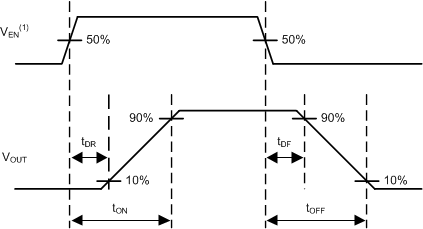
Rise and fall time of VEN is 100 ns.
Figure 2. Switching Characteristics Definitions