JAJSGO4D November   2018  – December 2019 TPS1HA08-Q1

PRODUCTION DATA.  

  1. 特長
  2. アプリケーション
  3. 概要
    1.     概略回路図
  4. 改訂履歴
  5. Device Comparison Table
  6. Pin Configuration and Functions
    1.     Pin Functions
    2. 6.1 Recommended Connections for Unused Pins
  7. Specifications
    1. 7.1 Absolute Maximum Ratings
    2. 7.2 ESD Ratings
    3. 7.3 Recommended Operating Conditions
    4. 7.4 Thermal Information
    5. 7.5 Electrical Characteristics
    6. 7.6 Switching Characteristics
    7. 7.7 SNS Timing Characteristics
    8. 7.8 Typical Characteristics
  8. Parameter Measurement Information
  9. Detailed Description
    1. 9.1 Overview
      1. 9.1.1 Device Nomenclature
    2. 9.2 Functional Block Diagram
    3. 9.3 Feature Description
      1. 9.3.1 Protection Mechanisms
        1. 9.3.1.1 Thermal Shutdown
        2. 9.3.1.2 Current Limit
          1. 9.3.1.2.1 Current Limit Foldback
          2. 9.3.1.2.2 Selectable Current Limit Threshold
          3. 9.3.1.2.3 Undervoltage Lockout (UVLO)
          4. 9.3.1.2.4 VBB during Short-to-Ground
        3. 9.3.1.3 Energy Limit
        4. 9.3.1.4 Voltage Transients
          1. 9.3.1.4.1 Load Dump
          2. 9.3.1.4.2 Driving Inductive and Capacitive Loads
        5. 9.3.1.5 Reverse Battery
        6. 9.3.1.6 Fault Event – Timing Diagrams
      2. 9.3.2 Diagnostic Mechanisms
        1. 9.3.2.1 VOUT Short-to-Battery and Open-Load
          1. 9.3.2.1.1 Detection With Switch Enabled
          2. 9.3.2.1.2 Detection With Switch Disabled
        2. 9.3.2.2 SNS Output
          1. 9.3.2.2.1 RSNS Value
            1. 9.3.2.2.1.1 High Accuracy Load Current Sense
            2. 9.3.2.2.1.2 SNS Output Filter
        3. 9.3.2.3 ST Pin
        4. 9.3.2.4 Fault Indication and SNS Mux
        5. 9.3.2.5 Resistor Sharing
        6. 9.3.2.6 High-Frequency, Low Duty-Cycle Current Sensing
      3. 9.3.3 Enable Watchdog
    4. 9.4 Device Functional Modes
      1. 9.4.1 Off
      2. 9.4.2 Standby
      3. 9.4.3 Diagnostic
      4. 9.4.4 Standby Delay
      5. 9.4.5 Active
      6. 9.4.6 Fault
  10. 10Application and Implementation
    1. 10.1 Application Information
      1. 10.1.1 Ground Protection Network
      2. 10.1.2 Interface With Microcontroller
      3. 10.1.3 I/O Protection
      4. 10.1.4 Inverse Current
      5. 10.1.5 Loss of GND
      6. 10.1.6 Automotive Standards
        1. 10.1.6.1 ISO7637-2
        2. 10.1.6.2 AEC – Q100-012 Short Circuit Reliability
      7. 10.1.7 Thermal Information
    2. 10.2 Typical Application
      1. 10.2.1 Design Requirements
      2. 10.2.2 Detailed Design Procedure
        1. 10.2.2.1 Thermal Considerations
        2. 10.2.2.2 Diagnostics
          1. 10.2.2.2.1 Selecting the RISNS Value
      3. 10.2.3 Application Curves
  11. 11Power Supply Recommendations
  12. 12Layout
    1. 12.1 Layout Guidelines
    2. 12.2 Layout Example
  13. 13デバイスおよびドキュメントのサポート
    1. 13.1 デバイス・サポート
      1. 13.1.1 関連資料
    2. 13.2 商標
    3. 13.3 静電気放電に関する注意事項
    4. 13.4 Glossary
  14. 14メカニカル、パッケージ、および注文情報

パッケージ・オプション

メカニカル・データ(パッケージ|ピン)
サーマルパッド・メカニカル・データ
発注情報

Voltage Transients

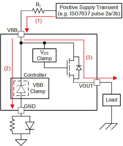
The contains two voltage clamps which protect the device against system-level voltage transients.

The clamp from VBB to GND is primarily used to protect the controller from positive transients on the supply line (for example, ISO7637-2). The clamp from VBB to VOUT is primarily used to limit the voltage across the FET when switching off an inductive load. Both clamp levels are set to protect the device during these fault conditions. If the voltage potential from VBB to GND exceeds the VBB clamp level, the clamp will allow current to flow through the device from VBB to GND (Path 2). If the voltage potential from VBB to VOUT exceeds VCLAMP, the power FET will allow current to flow from VBB to VOUT (Path 3).
TPS1HA08-Q1 vltg_trans_02_slvsd84.gifFigure 39. Current Path During Supply Voltage Transient