JAJSGO4D November   2018  – December 2019 TPS1HA08-Q1

PRODUCTION DATA.  

  1. 特長
  2. アプリケーション
  3. 概要
    1.     概略回路図
  4. 改訂履歴
  5. Device Comparison Table
  6. Pin Configuration and Functions
    1.     Pin Functions
    2. 6.1 Recommended Connections for Unused Pins
  7. Specifications
    1. 7.1 Absolute Maximum Ratings
    2. 7.2 ESD Ratings
    3. 7.3 Recommended Operating Conditions
    4. 7.4 Thermal Information
    5. 7.5 Electrical Characteristics
    6. 7.6 Switching Characteristics
    7. 7.7 SNS Timing Characteristics
    8. 7.8 Typical Characteristics
  8. Parameter Measurement Information
  9. Detailed Description
    1. 9.1 Overview
      1. 9.1.1 Device Nomenclature
    2. 9.2 Functional Block Diagram
    3. 9.3 Feature Description
      1. 9.3.1 Protection Mechanisms
        1. 9.3.1.1 Thermal Shutdown
        2. 9.3.1.2 Current Limit
          1. 9.3.1.2.1 Current Limit Foldback
          2. 9.3.1.2.2 Selectable Current Limit Threshold
          3. 9.3.1.2.3 Undervoltage Lockout (UVLO)
          4. 9.3.1.2.4 VBB during Short-to-Ground
        3. 9.3.1.3 Energy Limit
        4. 9.3.1.4 Voltage Transients
          1. 9.3.1.4.1 Load Dump
          2. 9.3.1.4.2 Driving Inductive and Capacitive Loads
        5. 9.3.1.5 Reverse Battery
        6. 9.3.1.6 Fault Event – Timing Diagrams
      2. 9.3.2 Diagnostic Mechanisms
        1. 9.3.2.1 VOUT Short-to-Battery and Open-Load
          1. 9.3.2.1.1 Detection With Switch Enabled
          2. 9.3.2.1.2 Detection With Switch Disabled
        2. 9.3.2.2 SNS Output
          1. 9.3.2.2.1 RSNS Value
            1. 9.3.2.2.1.1 High Accuracy Load Current Sense
            2. 9.3.2.2.1.2 SNS Output Filter
        3. 9.3.2.3 ST Pin
        4. 9.3.2.4 Fault Indication and SNS Mux
        5. 9.3.2.5 Resistor Sharing
        6. 9.3.2.6 High-Frequency, Low Duty-Cycle Current Sensing
      3. 9.3.3 Enable Watchdog
    4. 9.4 Device Functional Modes
      1. 9.4.1 Off
      2. 9.4.2 Standby
      3. 9.4.3 Diagnostic
      4. 9.4.4 Standby Delay
      5. 9.4.5 Active
      6. 9.4.6 Fault
  10. 10Application and Implementation
    1. 10.1 Application Information
      1. 10.1.1 Ground Protection Network
      2. 10.1.2 Interface With Microcontroller
      3. 10.1.3 I/O Protection
      4. 10.1.4 Inverse Current
      5. 10.1.5 Loss of GND
      6. 10.1.6 Automotive Standards
        1. 10.1.6.1 ISO7637-2
        2. 10.1.6.2 AEC – Q100-012 Short Circuit Reliability
      7. 10.1.7 Thermal Information
    2. 10.2 Typical Application
      1. 10.2.1 Design Requirements
      2. 10.2.2 Detailed Design Procedure
        1. 10.2.2.1 Thermal Considerations
        2. 10.2.2.2 Diagnostics
          1. 10.2.2.2.1 Selecting the RISNS Value
      3. 10.2.3 Application Curves
  11. 11Power Supply Recommendations
  12. 12Layout
    1. 12.1 Layout Guidelines
    2. 12.2 Layout Example
  13. 13デバイスおよびドキュメントのサポート
    1. 13.1 デバイス・サポート
      1. 13.1.1 関連資料
    2. 13.2 商標
    3. 13.3 静電気放電に関する注意事項
    4. 13.4 Glossary
  14. 14メカニカル、パッケージ、および注文情報

パッケージ・オプション

メカニカル・データ(パッケージ|ピン)
サーマルパッド・メカニカル・データ
発注情報

Driving Inductive and Capacitive Loads

When switching off an inductive load, the inductor may impose a negative voltage on the output of the switch. The includes a voltage clamp to limit voltage across the FET. The maximum acceptable load inductance is a function of the device robustness. With a 5 mH load, the can withstand a single pulse of 95 mJ inductive dissipation at 125°C and can withstand 56 mJ of inductive dissipation with a 10 Hz repetitive pulse. If the application parameters exceed this device limit, it is necessary to use a protection device like a freewheeling diode to dissipate the energy stored in the inductor. Figure 40 shows the discharging a 5 mH load that is driven at 5 A.
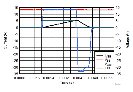
TPS1HA08-Q1 Inductive Repetitive.gifFigure 40. Inductive Discharge (5 mH, 5 A)

In addition, the current limit provides an ideal way to charge a capacitive load safely with limited inrush current. With no protection, charging a large capacitive load can lead to high inrush currents that pull a supply down, however by using the low current limit device options the capacitive load can be safely charged.

For more information on driving inductive or capacitive loads, reference TI's "How To Drive Inductive, Capacitive, and Lighting Loads with Smart High Side Switch application report.