JAJSUS5 June   2024 TPS1HTC100-Q1

PRODUCTION DATA  

  1.   1
  2. 特長
  3. アプリケーション
  4. 概要
  5. Pin Configuration and Functions
    1. 4.1 Recommended Connections for Unused Pins
  6. Specifications
    1. 5.1 Absolute Maximum Ratings
    2. 5.2 ESD Ratings
    3. 5.3 Recommended Operating Conditions
    4. 5.4 Thermal Information
    5. 5.5 Electrical Characteristics
    6. 5.6 SNS Timing Characteristics
    7. 5.7 Switching Characteristics
    8. 5.8 Timing Diagrams
    9. 5.9 Typical Characteristics
  7. Parameter Measurement Information
  8. Detailed Description
    1. 7.1 Overview
    2. 7.2 Functional Block Diagram
    3. 7.3 Feature Description
      1. 7.3.1 Accurate Current Sense
      2. 7.3.2 Programmable Current Limit
        1. 7.3.2.1 Capacitive Charging
      3. 7.3.3 Inductive-Load Switching-Off Clamp
      4. 7.3.4 Full Protections and Diagnostics
        1. 7.3.4.1 Short-Circuit and Overload Protection
        2. 7.3.4.2 Open-Load Detection
        3. 7.3.4.3 Thermal Protection Behavior
        4. 7.3.4.4 UVLO Protection
        5. 7.3.4.5 Reverse Polarity Protection
        6. 7.3.4.6 Protection for MCU I/Os
      5. 7.3.5 Diagnostic Enable Function
    4. 7.4 Device Functional Modes
      1. 7.4.1 Device Functional Modes
  9. Application and Implementation
    1. 8.1 Application Information
    2. 8.2 Typical Application
      1. 8.2.1 Design Requirements
      2. 8.2.2 Detailed Design Procedure
        1. 8.2.2.1 Dynamically Changing Current Limit
    3. 8.3 Power Supply Recommendations
    4. 8.4 Layout
      1. 8.4.1 Layout Guidelines
      2. 8.4.2 Layout Example
        1. 8.4.2.1 Without a GND Network
        2. 8.4.2.2 With a GND Network
        3. 8.4.2.3 Thermal Considerations
  10. Device and Documentation Support
    1. 9.1 Documentation Support
      1. 9.1.1 Related Documentation
    2. 9.2 ドキュメントの更新通知を受け取る方法
    3. 9.3 サポート・リソース
    4. 9.4 Trademarks
    5. 9.5 静電気放電に関する注意事項
    6. 9.6 用語集
  11. 10Revision History
  12. 11Mechanical, Packaging, and Orderable Information

パッケージ・オプション

メカニカル・データ(パッケージ|ピン)
サーマルパッド・メカニカル・データ
発注情報

Timing Diagrams

TPS1HTC100-Q1 Switching Characteristics Definitions
Rise and fall time of VEN is 100ns.
Figure 5-1 Switching Characteristics Definitions
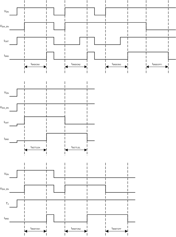
TPS1HTC100-Q1 SNS Timing Characteristics Definitions
Rise and fall times of control signals are 100ns. Control signals include: EN, DIA_EN.
Figure 5-2 SNS Timing Characteristics Definitions