JAJSCP5 December 2016 TPS2069D
PRODUCTION DATA.
11 Layout
11.1 Layout Guidelines
- Place the 100-nF bypass capacitor near the IN and GND pins, and make the connections using a low inductance trace.
- Place at least 10-µF low ESR ceramic capacitor near the OUT and GND pins, and make the connections using a low inductance trace.
- The PowerPAD™ should be directly connected to PCB ground plane using wide and short copper trace.
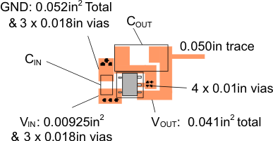
11.2 Layout Example
 Figure 26. DBV Package PCB Layout Example
11.3 Power Dissipation and Junction Temperature
It is good design practice to estimate power dissipation and maximum expected junction temperature of the TPS2069D. The system designer can control choices of package, proximity to other power dissipating devices, and printed-circuit-board (PCB) design based on these calculations. These have a direct influence on maximum junction temperature. Other factors, such as airflow and maximum ambient temperature, are often determined by system considerations. It is important to remember that these calculations do not include the effects of adjacent heat sources, and enhanced or restricted air flow.
Addition of extra PCB copper area around these devices is recommended to reduce the thermal impedance and maintain the junction temperature as low as practical. The lower junction temperatures achieved by soldering the pad improve the efficiency and reliability of both device parts and the system. The following examples were used to determine the θJACustom thermal impedances noted in Thermal Information. They were based on use of the JEDEC high-k circuit board construction (2 signal and 2 plane) with 4, 1-oz. copper weight, layers.
As shown in Equation 1, the following procedure requires iteration because power loss is due to the internal MOSFET I2 × RDS(ON), and RDS(ON) is a function of the junction temperature. As an initial estimate, use the RDS(ON) at 125°C from the Typical Characteristics, and the preferred package thermal resistance for the preferred board construction from the Thermal Information table.
where
- IOUT = rated OUT pin current (A)
- RDS(ON) = Power switch on-resistance at an assumed TJ (Ω)
- TA = Maximum ambient temperature (°C)
- TJ = Maximum junction temperature (°C)
- θJA = Thermal resistance (°C/W)
If the calculated TJ is substantially different from the original assumption, estimate a new value of RDS(ON) using the typical characteristic plot and recalculate.
If the resulting TJ is not less than 125°C, try a PCB construction and/or package with lower θJA.