SBVS124A November 2008 – May 2016 TPS2115A-Q1
PRODUCTION DATA.
- 1 Features
- 2 Applications
- 3 Description
- 4 Revision History
- 5 Pin Configuration and Functions
- 6 Specifications
- 7 Parameter Measurement Information
- 8 Detailed Description
- 9 Application and Information
- 10Power Supply Recommendations
- 11Layout
- 12Device and Documentation Support
- 13Mechanical, Packaging, and Orderable Information
8 Detailed Description
8.1 Overview
The TPS2115A-Q1 power multiplexer enables seamless transition between two power supplies, such as a two supply rails or a battery and AC-to-DC wall adapter. Each supply operates at 2.8 V to 5.5 V and the output can deliver up to 1 A. The TPS2115A-Q1 device includes extensive protection circuitry including user-programmable current limiting, thermal protection, inrush current control, seamless supply transition, cross-conduction blocking, and reverse-conduction blocking. These features greatly simplify designing power multiplexer applications.
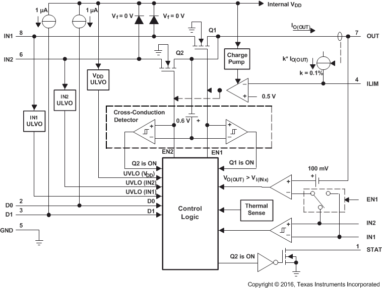
8.2 Functional Block Diagram

8.3 Feature Description
8.3.1 N-Channel MOSFETs
Two internal high-side power MOSFETs implement a single-pole double-throw (SPDT) switch. Digital logic selects the IN1 switch, IN2 switch, or no switch (Hi-Z state). The MOSFETs have no parallel diodes so output-to-input current cannot flow when the FET is off. An integrated comparator prevents turn-on of a FET switch if the output voltage is greater than the input voltage.
8.3.2 Cross-Conduction Blocking
The switching circuitry ensures that both power switches never conducts at the same time. A comparator monitors the gate-to-source voltage of each power FET and allows a FET to turn on only if the gate-to-source voltage of the other FET is below the turn-on threshold voltage.
8.3.3 Reverse-Conduction Blocking
When the TPS2115A-Q1 device switches from a higher-voltage supply to a lower-voltage supply, current can potentially flow back from the load capacitor into the lower-voltage supply. To minimize such reverse conduction, the TPS2115A-Q1 device does not connect a supply to the output until the output voltage has fallen to within 100 mV of the supply voltage. Once a supply has been connected to the output, the supply remains connected regardless of output voltage.
8.3.4 Charge Pump
The higher voltage of supplies IN1 and IN2 powers the internal charge pump. The charge pump provides power to the current-limit amplifier and allows the output FET gate voltage to be higher than the IN1 and IN2 supply voltages. A gate voltage that is higher than the source voltage is necessary to turn on the N-channel FET.
8.3.5 Current Limiting
A resistor RILIM from ILIM to GND sets the current limit to ( ( 500 Ω ) / RILIM ) A. It is recommended to keep the current limit set to 1.25 A or lower (RILIM ≥ 400 Ω). Setting resistor RILIM equal to zero is not recommended as that disables current limiting.
8.3.6 Output Voltage Slew-Rate Control
The TPS2115A-Q1 device slews the output voltage at a slow rate when OUT switches to IN1 or IN2 from the Hi-Z state (see Table 1). A slow slew rate limits the inrush current into the load capacitor. High inrush currents can glitch the voltage bus and cause a system to hang up or reset. It can also cause reliability issues such as pitting the connector power contacts when hot-plugging a load such as a PCI card. The TPS2115A-Q1 device slews the output voltage at a much faster rate when OUT switches between IN1 and IN2. The fast rate minimizes the output voltage droop and reduces the output voltage hold-up capacitance requirement.
8.4 Device Functional Modes
Table 1 is the Truth Table for the TPS2115A-Q1 power multiplexer.
Table 1. Truth Table
| D1 | D0 | VI(IN2) > VI(IN1) (1) | STAT | OUT(2) |
|---|---|---|---|---|
| 0 | 0 | X | Hi-Z | IN2 |
| 0 | 1 | No | 0 | IN1 |
| 0 | 1 | Yes | Hi-Z | IN2 |
| 1 | 0 | X | 0 | IN1 |
| 1 | 1 | X | 0 | Hi-Z |
8.4.1 Auto-Switching Mode
D0 equal to logic 1 and D1 equal to logic 0 selects the auto-switching mode. In this mode, OUT connects to the higher of IN1 and IN2.
8.4.2 Manual Switching Mode
D0 equal to logic 0 selects the manual-switching mode. In this mode, OUT connects to IN1 if D1 is equal to logic 1, otherwise OUT connects to IN2.