SBVS124A November 2008 – May 2016 TPS2115A-Q1
PRODUCTION DATA.
- 1 Features
- 2 Applications
- 3 Description
- 4 Revision History
- 5 Pin Configuration and Functions
- 6 Specifications
- 7 Parameter Measurement Information
- 8 Detailed Description
- 9 Application and Information
- 10Power Supply Recommendations
- 11Layout
- 12Device and Documentation Support
- 13Mechanical, Packaging, and Orderable Information
6 Specifications
6.1 Absolute Maximum Ratings
over operating free-air temperature range (unless otherwise noted)(1)(2)| MIN | MAX | UNIT | |||
|---|---|---|---|---|---|
| VI | Input voltage range | IN1, IN2, D0, D1, ILIM | –0.3 | 6 | V |
| VO | Output voltage range | OUT, STAT | –0.3 | 6 | V |
| IO(sink) | Output sink current | STAT | 5 | mA | |
| IO | Continuous output current | OUT | 1.5 | A | |
| PD | Continuous total-power dissipation | See Thermal Information | |||
| TA | Operating free-air temperature range | –40 | 85 | °C | |
| TJ | Operating virtual-junction temperature range | –40 | 125 | °C | |
| Tlead | Lead temperature soldering | 1,6 mm (1/16 inch) from case for 10 seconds | 260 | °C | |
| Storage temperature, Tstg | –65 | 150° | °C | ||
(1) Stresses beyond those listed under Absolute Maximum Ratings may cause permanent damage to the device. These are stress ratings only, which do not imply functional operation of the device at these or any other conditions beyond those indicated under Recommended Operating Conditions. Exposure to absolute-maximum-rated conditions for extended periods may affect device reliability.
(2) All voltages are with respect to GND.
6.2 ESD Ratings
| VALUE | UNIT | |||
|---|---|---|---|---|
| V(ESD) | Electrostatic discharge | Human-body model (HBM) | ±2000 | V |
| Charged-device model (CDM) | ±500 | |||
6.3 Recommended Operating Conditions
| MIN | NOM | MAX | UNIT | ||||
|---|---|---|---|---|---|---|---|
| VI | Input voltage | IN1 | VI(IN2) ≥ 2.8 V | 1.5 | 5.5 | V | |
| VI(IN2) < 2.8 V | 2.8 | 5.5 | |||||
| IN2 | VI(IN1) ≥ 2.8 V | 1.5 | 5.5 | ||||
| VI(IN1) < 2.8 V | 2.8 | 5.5 | |||||
| D0, D1 | 0 | 5.5 | |||||
| VIH | High-level input voltage | D0, D1 | 2 | V | |||
| VIL | Low-level input voltage | D0, D1 | 0.7 | V | |||
| IO | Current limit adjustment range | OUT | 0.63 | 1.25 | A | ||
| TA | Operating free-air temperature | –40 | 85 | °C | |||
| TJ | Operating virtual-junction temperature range | –40 | 125 | °C | |||
6.4 Thermal Information
| THERMAL METRIC(1) | TPS2115A-Q1 | UNIT | |
|---|---|---|---|
| PW (TSSOP) | |||
| 8 PINS | |||
| RθJA | Junction-to-ambient thermal resistance | 159.2 | °C/W |
| RθJC(top) | Junction-to-case (top) thermal resistance | 40.7 | °C/W |
| RθJB | Junction-to-board thermal resistance | 90.1 | °C/W |
| ψJT | Junction-to-top characterization parameter | 2.1 | °C/W |
| ψJB | Junction-to-board characterization parameter | 87.8 | °C/W |
| RθJC(bot) | Junction-to-case (bottom) thermal resistance | n/a | °C/W |
(1) For more information about traditional and new thermal metrics, see the Semiconductor and IC Package Thermal Metrics application report, SPRA953.
6.5 Electrical Characteristics
over operating free-air temperature range, VI(IN1) = VI(IN2) = 5.5 V, RILIM = 400 Ω (unless otherwise noted)| PARAMETER | TEST CONDITIONS | MIN | TYP | MAX | UNIT | ||
|---|---|---|---|---|---|---|---|
| POWER SWITCH (1) | |||||||
| rDS(on) | Drain-source on-state resistance (INx to OUT) | TA = 25°C, IL = 500 mA | VI(IN1) = VI(IN2) = 5.0 V | 84 | 110 | mΩ | |
| VI(IN1) = VI(IN2) = 3.3 V | 84 | 110 | |||||
| VI(IN1) = VI(IN2) = 2.8 V | 84 | 110 | |||||
| TA = 85°C, IL = 500 mA | VI(IN1) = VI(IN2) = 5.0 V | 150 | |||||
| VI(IN1) = VI(IN2) = 3.3 V | 150 | ||||||
| VI(IN1) = VI(IN2) = 2.8 V | 150 | ||||||
| LOGIC INPUTS (D0 AND D1) | |||||||
| II | Input current at D0 or D1 | D0 or D1 = high, sink current | 1 | μA | |||
| D0 or D1 = low, source current | 0.5 | 1.4 | 5 | ||||
| SUPPLY AND LEAKAGE CURRENTS | |||||||
| Supply current from IN1 (operating) | D1 = high, D0 = low (IN1 active), VI(IN1) = 5.5 V, VI(IN2) = 3.3 V, IO(OUT) = 0 A | 55 | 90 | μA | |||
| D1 = high, D0 = low (IN1 active), VI(IN1) = 3.3 V, VI(IN2) = 5.5 V, IO(OUT) = 0 A | 1 | 12 | |||||
| D0 = D1 = low (IN2 active), VI(IN1) = 5.5 V, VI(IN2) = 3.3 V, IO(OUT) = 0 A | 75 | ||||||
| D0 = D1 = low (IN2 active), VI(IN1) = 3.3 V, VI(IN2) = 5.5 V, IO(OUT) = 0 A | 1 | ||||||
| Supply current from IN2 (operating) | D1 = high, D0 = low (IN1 active), VI(IN1) = 5.5 V, VI(IN2) = 3.3 V, IO(OUT) = 0 A | 1 | μA | ||||
| D1 = high, D0 = low (IN1 active), VI(IN1) = 3.3 V, VI(IN2) = 5.5 V, IO(OUT) = 0 A | 75 | ||||||
| D0 = D1 = low (IN2 active), VI(IN1) = 5.5 V, VI(IN2) = 3.3 V, IO(OUT) = 0 A | 1 | 12 | |||||
| D0 = D1 = low (IN2 active), VI(IN1) = 3.3 V, VI(IN2) = 5.5 V, IO(OUT) = 0 A | 55 | 90 | |||||
| Quiescent current from IN1 (standby) | D0 = D1 = high (inactive), IO(OUT) = 0 A | VI(IN1) = 5.5 V, VI(IN2) = 3.3 V | 0.5 | 2 | μA | ||
| VI(IN1) = 3.3 V, VI(IN2) = 5.5 V | 1 | ||||||
| Quiescent current from IN2 (standby) | D0 = D1 = high (inactive), IO(OUT) = 0 A | VI(IN1) = 5.5 V, VI(IN2) = 3.3 V | 1 | μA | |||
| VI(IN1) = 3.3 V, VI(IN2) = 5.5 V | 0.5 | 2 | |||||
| Forward leakage current from IN1 (measured from OUT to GND) | D0 = D1 = high (inactive), VI(IN1) = 5.5 V, IN2 open, VO(OUT) = 0 V (shorted), TA = 25°C |
0.1 | 5 | μA | |||
| Forward leakage current from IN2 (measured from OUT to GND) | D0 = D1= high (inactive), VI(IN2) = 5.5 V, IN1 open, VO(OUT) = 0 V (shorted), TA = 25°C |
0.1 | 5 | μA | |||
| Reverse leakage current to INx (measured from INx to GND) | D0 = D1 = high (inactive), VI(INx) = 0 V, VO(OUT) = 5.5 V, TA = 25°C | 0.3 | 5 | μA | |||
| CURRENT LIMIT CIRCUIT | |||||||
| Current limit accuracy | RILIM = 400 Ω | 0.95 | 1.25 | 1.56 | A | ||
| RILIM = 700 Ω | 0.47 | 0.71 | 0.99 | ||||
| td | Current limit settling time | Time for short-circuit output current to settle within 10% of its steady state value | 1 | ms | |||
| II | Input current at ILIM | VI(ILIM) = 0 V, IO(OUT) = 0 A | –15 | 0 | μA | ||
| UVLO | |||||||
| IN1 and IN2 UVLO | Falling edge | 1.15 | 1.25 | V | |||
| Rising edge | 1.30 | 1.35 | |||||
| IN1 and IN2 UVLO hysteresis | 30 | 57 | 65 | mV | |||
| Internal VDD UVLO (the higher of IN1 and IN2) | Falling edge | 2.4 | 2.53 | V | |||
| Rising edge | 2.58 | 2.8 | |||||
| Internal VDD UVLO hysteresis | 30 | 50 | 75 | mV | |||
| UVLO deglitch for IN1, IN2 | Falling edge | 110 | μs | ||||
| REVERSE CONDUCTION BLOCKING | |||||||
| ΔVIO(blk) | Minimum input-to-output voltage difference to block switching | D0 = D1 = high, VI(INx) = 3.3 V. Connect OUT to a 5-V supply through a series 1-kΩ resistor. Set D0 = low. Slowly decrease the supply voltage until OUT connects to IN1. | 80 | 100 | 120 | mV | |
| THERMAL SHUTDOWN | |||||||
| Thermal shutdown threshold | TPS2115A-Q1 device is in current limit. | 135 | °C | ||||
| Recovery from thermal shutdown | TPS2115A-Q1 device is in current limit. | 125 | °C | ||||
| Hysteresis | 10 | °C | |||||
| IN2-IN1 COMPARATORS | |||||||
| Hysteresis of IN2-IN1 comparator | 0.1 | 0.2 | V | ||||
| Deglitch of IN2-IN1 comparator (both ↑↓) |
10 | 20 | 50 | μs | |||
| STAT OUTPUT | |||||||
| Ileak | Leakage current | VO(STAT) = 5.5 V | 0.01 | 1 | μA | ||
| Vsat | Saturation voltage | II(STAT) = 2 mA, IN1 switch is on | 0.13 | 0.4 | V | ||
| td | Deglitch time (falling edge only) |
150 | μs | ||||
(1) The TPS2115A-Q1 device can switch a voltage as low as 1.5 V as long as there is a minimum of 2.8 V at one of the input power pins. In this case, the lower supply voltage has no effect on the IN1 and IN2 switch on-resistances.
6.6 Switching Characteristics
over operating free-air temperature range, VI(IN1) = VI(IN2) = 5.5 V, RILIM = 400 Ω (unless otherwise noted)| PARAMETER | TEST CONDITIONS | MIN | TYP | MAX | UNIT | ||
|---|---|---|---|---|---|---|---|
| Power Switch | |||||||
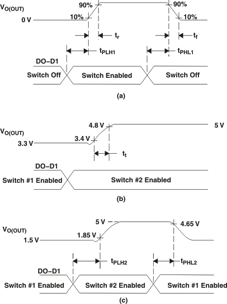
| tr | Output rise time from an enable | VI(IN1) = VI(IN2) = 5 V | TA = 25°C, CL = 1 μF, IL = 500 mA, See Figure 1(a) | 1 | 1.8 | 3 | ms |
| tf | Output fall time from a disable | VI(IN1) = VI(IN2) = 5 V | TA = 25°C, CL = 1 μF, IL = 500 mA, See Figure 1(a) | 0.5 | 1 | 2 | ms |
| tt | Transition time | IN1 to IN2 transition, VI(IN1) = 3.3 V, VI(IN2) = 5 V |
TA = 85°C, CL = 10 μF, IL = 500 mA [Measure transition time as 10%-90% rise time or from 3.4 V to 4.8 V on VO(OUT)], See Figure 1(b) | 40 | 60 | μs | |
| IN2 to IN1 transition, VI(IN1) = 5 V, VI(IN2) = 3.3 V |
40 | 60 | |||||
| tPLH1 | Turn-on propagation delay from enable | VI(IN1) = VI(IN2) = 5 V, Measured from enable to 10% of VO(OUT) | TA = 25°C, CL = 10 μF, IL = 500 mA, See Figure 1(a) | 1 | ms | ||
| tPHL1 | Turn-off propagation delay from a disable | VI(IN1) = VI(IN2) = 5 V, Measured from disable to 90% of VO(OUT) | TA = 25°C, CL = 10 μF, IL = 500 mA, See Figure 1(a) | 5 | ms | ||
| tPLH2 | Switch-over rising propagation delay | Logic 1 to Logic 0 transition on D1, VI(IN1) = 1.5 V, VI(IN2) = 5 V, VI(D0) = 0 V, Measured from D1 to 10% of VO(OUT) | TA = 25°C, CL = 10 μF, IL = 500 mA, See Figure 1(c) | 40 | 100 | μs | |
| tPHL2 | Switch-over falling propagation delay | Logic 0 to Logic 1 transition on D1, VI(IN1) = 1.5 V, VI(IN2) = 5 V, VI(D0) = 0 V, Measured from D1 to 90% of VO(OUT) | TA = 25°C, CL = 10 μF, IL = 500 mA, See Figure 1(c) | 2 | 5 | 10 | ms |
6.7 Typical Characteristics
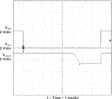
| Input to D1: f=28 Hz, 78% Duty Cycle | See Figure 14 for test circuit | |
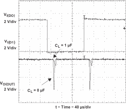
| Input to D1: f = 580 Hz, 90% duty cycle | See Figure 16 for test circuit | |
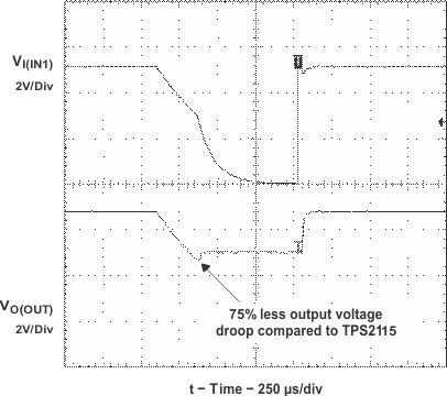
| Input to IN1 through switch: f = 220 Hz, 20% duty cycle | See Figure 18 for test circuit | |
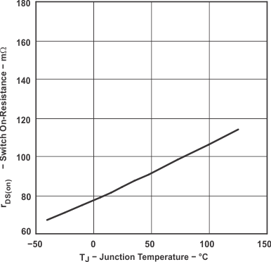
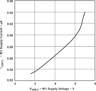
| VI(IN2) = 0 V | IO(OUT) = 0 A |
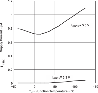
| VI(IN1) = 5.5 V | VI(IN2) = 3.3 V | IO(OUT) = 0 A |
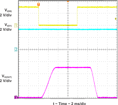
| Input to D0: f=28 Hz, 78% Duty Cycle | See Figure 15 for test circuit | |
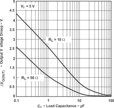
| Input to D1: f = 28 Hz, 50% duty cycle | See Figure 17 for test circuit | |
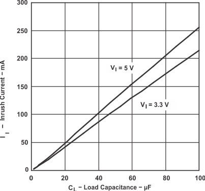
| Input to D0: f=28 Hz 90% duty cycle | See Figure 19 for test circuit | |
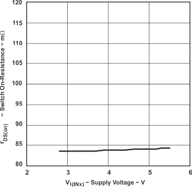
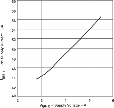
| VI(IN2) = 0 V | IO(OUT) = 0 A |
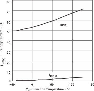
| VI(IN1) = 5.5 V | VI(IN2) = 3.3 V | IO(OUT) = 0 A |
