SLVSFL4 June   2020 TPS2124

PRODUCTION DATA.  

  1. Features
  2. Applications
  3. Description
    1.     Device Images
      1.      Typical Application
  4. Revision History
  5. Pin Configuration and Functions
    1.     Pin Functions
  6. Specifications
    1. 6.1 Absolute Maximum Ratings
    2. 6.2 ESD Ratings
    3. 6.3 Recommended Operating Conditions
    4. 6.4 Thermal Information
    5. 6.5 Electrical Characteristics
    6. 6.6 Typical Characteristics
  7. Parameter Measurement Information
  8. Detailed Description
    1. 8.1 Overview
    2. 8.2 Functional Block Diagram
    3. 8.3 Feature Description
      1. 8.3.1 Input Settling Time and Output Soft Start Control (SS)
        1. 8.3.1.1 Slew Rate vs. CSS Capacitor
      2. 8.3.2 Active Current Limiting (ILM)
      3. 8.3.3 Short-Circuit Protection
      4. 8.3.4 Thermal Protection (TSD)
      5. 8.3.5 Over-voltage Protection (OVx)
      6. 8.3.6 Fast Reverse Current Blocking (RCB)
      7. 8.3.7 Input Voltage Comparator (VCOMP)
    4. 8.4 TPS2124 Device Functional Modes
  9. Application and Implementation
    1. 9.1 Application Information
    2. 9.2 Typical Application
      1. 9.2.1 Manual Switchover Schematic
      2. 9.2.2 Design Requirements
      3. 9.2.3 Detailed Design Description
      4. 9.2.4 Design Procedure
        1. 9.2.4.1 Selecting OVx Resistors
        2. 9.2.4.2 Selecting Soft-Start Capacitor and Current Limit Resistors
      5. 9.2.5 Application Curves
    3. 9.3 Highest Voltage Operation (VCOMP)
      1. 9.3.1 Application Schematic
      2. 9.3.2 Design Requirements
      3. 9.3.3 Detailed Design Description
      4. 9.3.4 Detailed Design Procedure
      5. 9.3.5 Application Curves
    4. 9.4 Reverse Polarity Protection with TPS2124
  10. 10Power Supply Recommendations
  11. 11Layout
    1. 11.1 Layout Guidelines
    2. 11.2 Layout Example
  12. 12Device and Documentation Support
    1. 12.1 Receiving Notification of Documentation Updates
    2. 12.2 Support Resources
    3. 12.3 Trademarks
    4. 12.4 Electrostatic Discharge Caution
    5. 12.5 Glossary
  13. 13Mechanical, Packaging, and Orderable Information

パッケージ・オプション

メカニカル・データ(パッケージ|ピン)
サーマルパッド・メカニカル・データ
発注情報

Typical Characteristics

TPS2124 D002_SLVSEA3.gif
ILM = 1.5A
Figure 1. Quiescent Current vs Input Voltage
TPS2124 D006_SLVSEA3.gif
VIN1 > UVLO VIN2 = 0V
Figure 3. Output Slew Rate vs CSS Capacitor
TPS2124 D004_SLVSEA3.gif
ILM = 1.5A
Figure 2. Standby Current vs Input Voltage
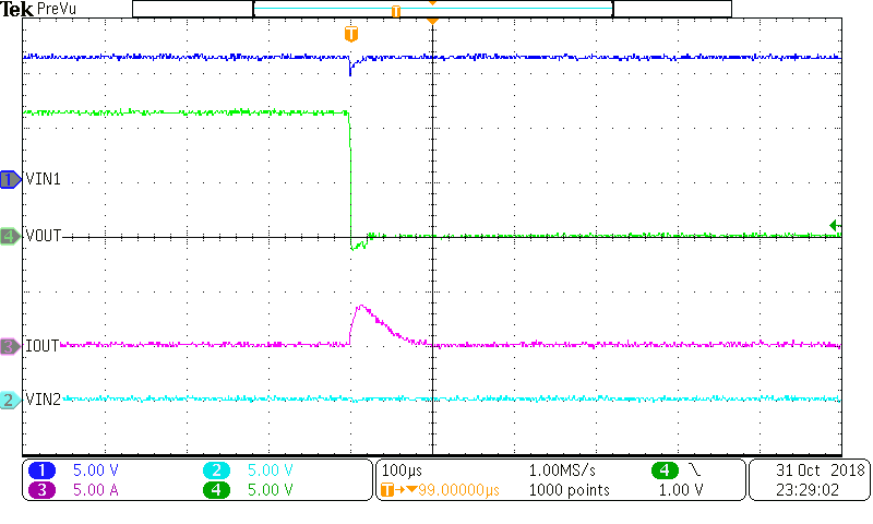
TPS2124 tek00000.png
VIN1 = 12 V VIN2 = 0 V
Figure 4. Hot Short on OUT while IN1 is Enabled
TPS2124 tek00001.jpg
VIN1 = 12 V VIN2 = 0 V VOUT = GND
RILM = 71.5kΩ
Figure 5. TPS2124 IN1 is Enabled with a Short on OUT