JAJSOD0A April 2022 – July 2022 TPS22811
PRODUCTION DATA
- 1 特長
- 2 アプリケーション
- 3 概要
- 4 Revision History
- 5 Pin Configuration and Functions
- 6 Specifications
-
7 Detailed Description
- 7.1 Overview
- 7.2 Functional Block Diagram
- 7.3
Feature Description
- 7.3.1 Undervoltage Lockout (UVLO and UVP)
- 7.3.2 Overvoltage Lockout (OVLO)
- 7.3.3 Inrush Current, Overcurrent, and Short-Circuit Protection
- 7.3.4 Analog Load Current Monitor
- 7.3.5 Overtemperature Protection (OTP)
- 7.3.6 Fault Response
- 7.3.7 Power-Good Indication (PG)
- 7.3.8 Quick Output Discharge (QOD)
- 7.4 Device Functional Modes
- 8 Application and Implementation
- 9 Power Supply Recommendations
- 10Layout
- 11Device and Documentation Support
- 12Mechanical, Packaging, and Orderable Information
6.8 Typical Characteristics
Figure 6-2 ON-Resistance vs Supply Voltage (TA = 25°C)
Figure 6-4 IN Quiescent Current vs Temperature
Figure 6-6 IN Shutdown Current vs Temperature
Figure 6-8 EN/UVLO Rising Threshold
vs Temperature
Figure 6-10 EN/UVLO Shutdown Falling Threshold vs Temperature
Figure 6-12 EN/OVLO Falling Threshold vs Temperature
Figure 6-14 Analog Current Monitor Gain Accuracy
Figure 6-16 PG Pin Voltage vs Temperature (VIN = 0 V)
Figure 6-18 PGTH Falling Threshold vs Temperature
Figure 6-20 Quick Output Discharge Resistance vs Temperature
Figure 6-22 Time to Thermal Shutdown During
Steady-State
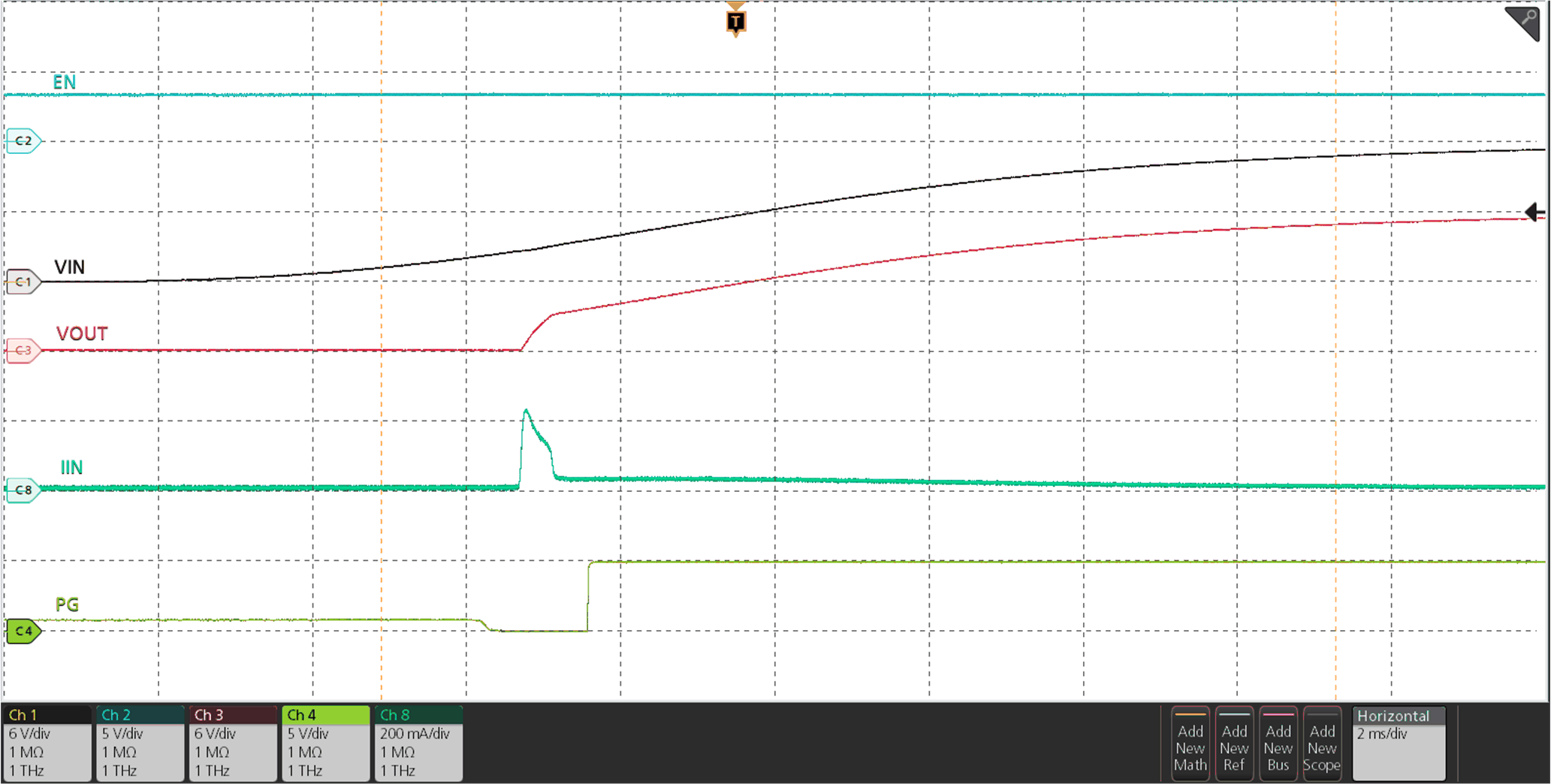
| VEN/UVLO = 3.3 V, COUT = 10 μF, CdVdt = Open, VIN ramped up to 12 V |
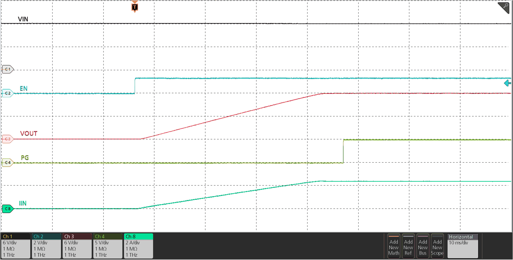
| VIN = 12 V, COUT = 220 μF, ROUT = 5 Ω, CdVdt = 3300 pF, VEN/UVLO stepped up to 1.4 V |
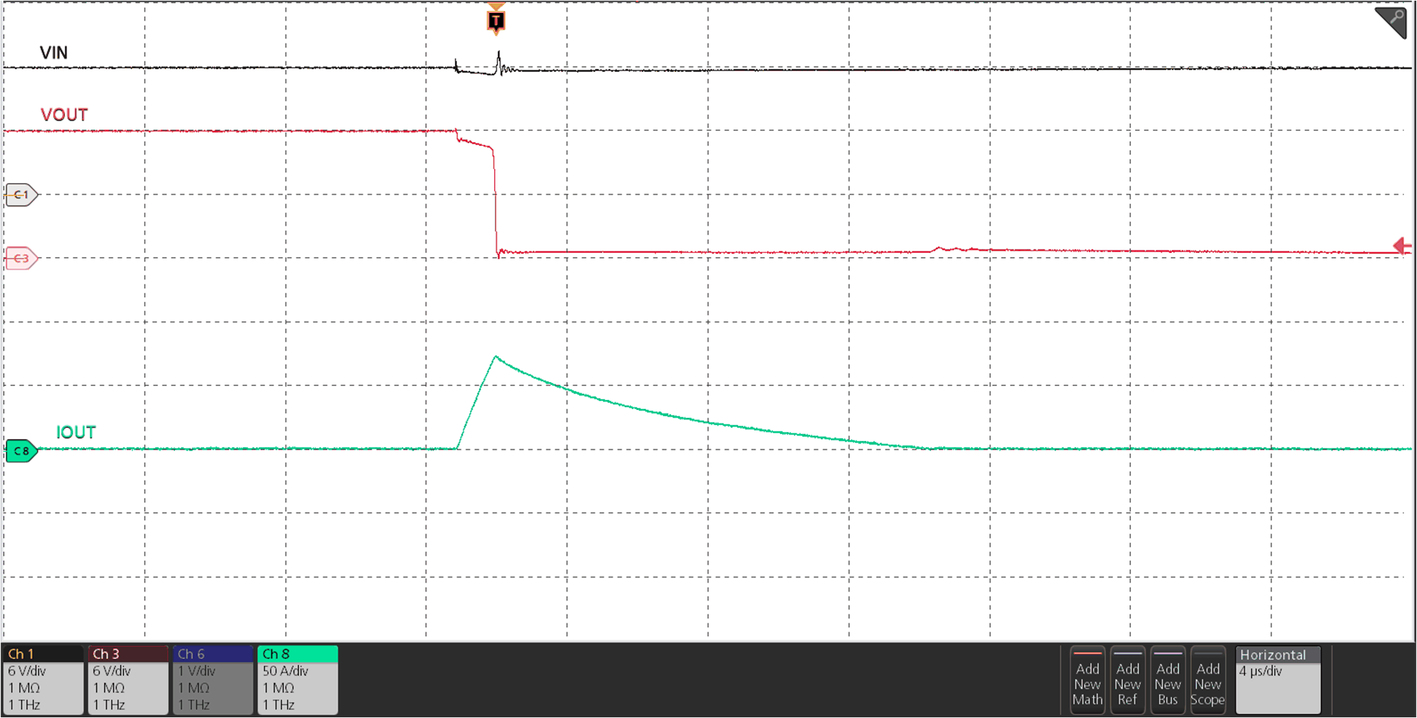
| VIN = 12 V, OUT stepped from open → short circuit to GND |
Figure 6-3 ON-Resistance vs Temperature (IOUT = 3 A)
Figure 6-5 IN OFF State (UVLO) Current vs Temperature
Figure 6-7 IN Undervoltage Threshold vs Temperature
Figure 6-9 EN/UVLO Falling Threshold vs Temperature
Figure 6-11 EN/OVLO Rising Threshold vs Temperature
Figure 6-13 Fixed Fast-Trip Threshold vs Temperature
Figure 6-15 DVDT Charging Current vs Temperature
Figure 6-17 PGTH Rising Threshold vs Temperature
Figure 6-19 PGTH Pin Leakage Current vs Temperature
Figure 6-21 Time to Thermal Shutdown During Inrush State
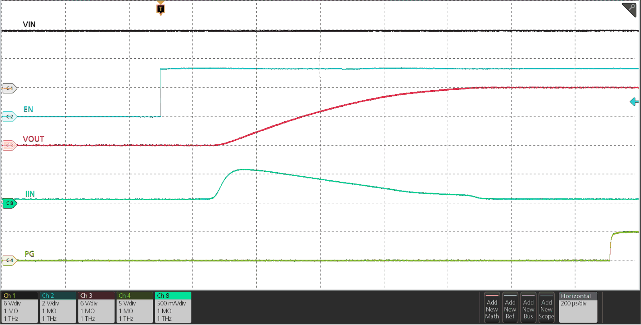
| VIN = 12 V, COUT = 10 μF, CdVdt = Open, VEN/UVLO stepped up to 3.3 V |
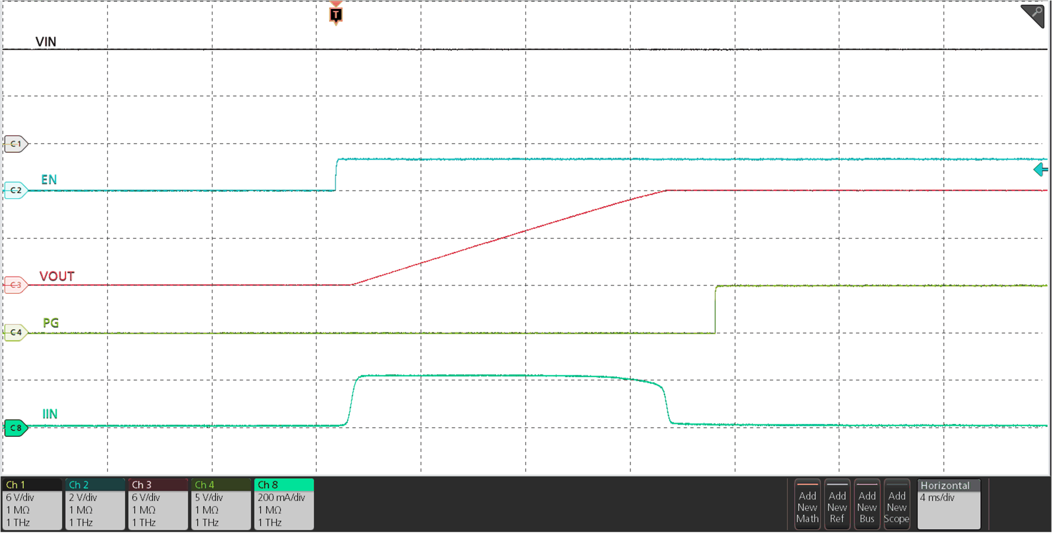
| VIN = 12 V, COUT = 220 μF, CdVdt = 3300 pF, VEN/UVLO stepped up to 1.4 V |
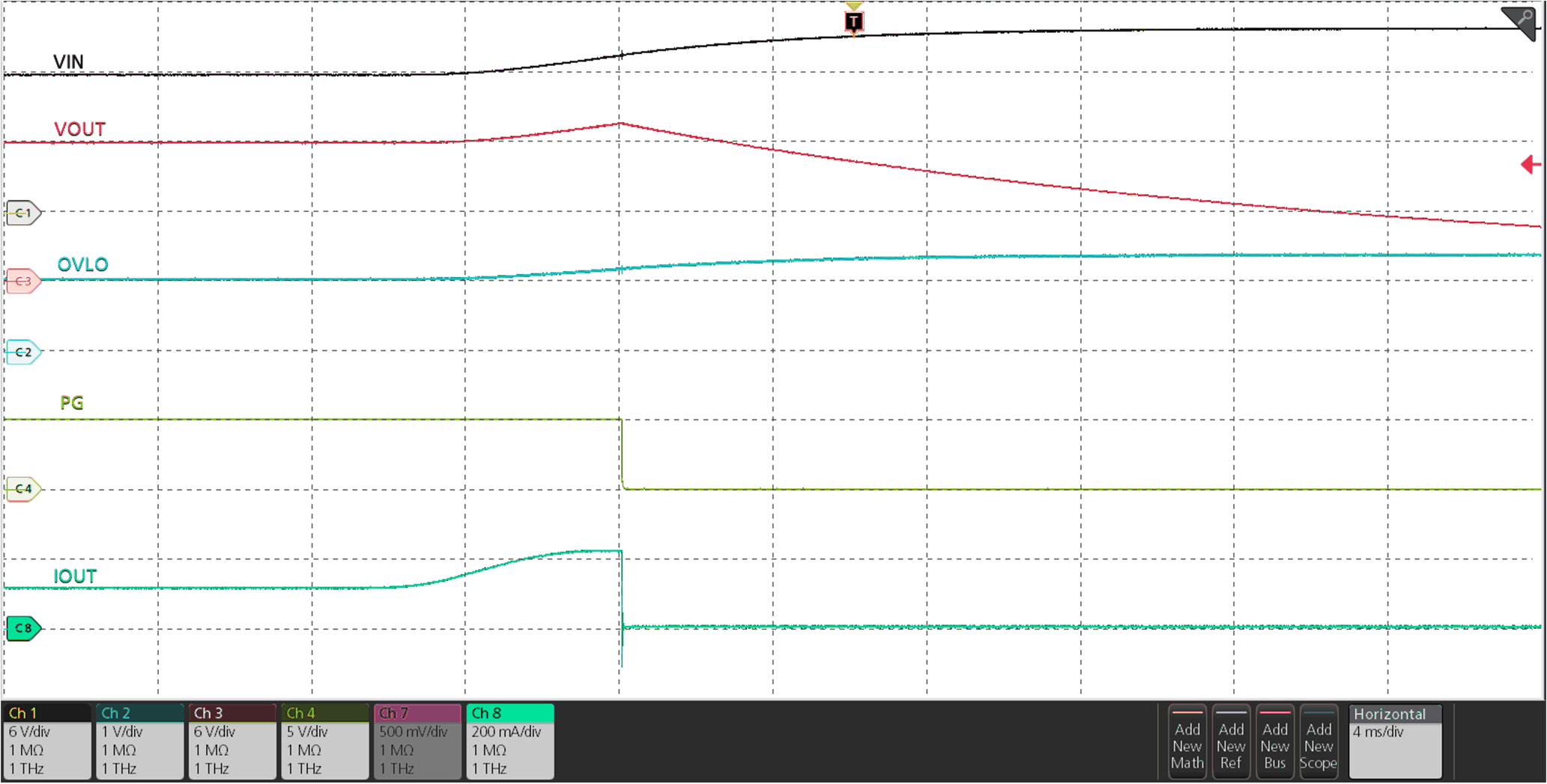
| VIN Overvoltage threshold set to 13.6 V using resistor ladder connected on OVLO pin, VIN ramped up from 12 V to 16 V |
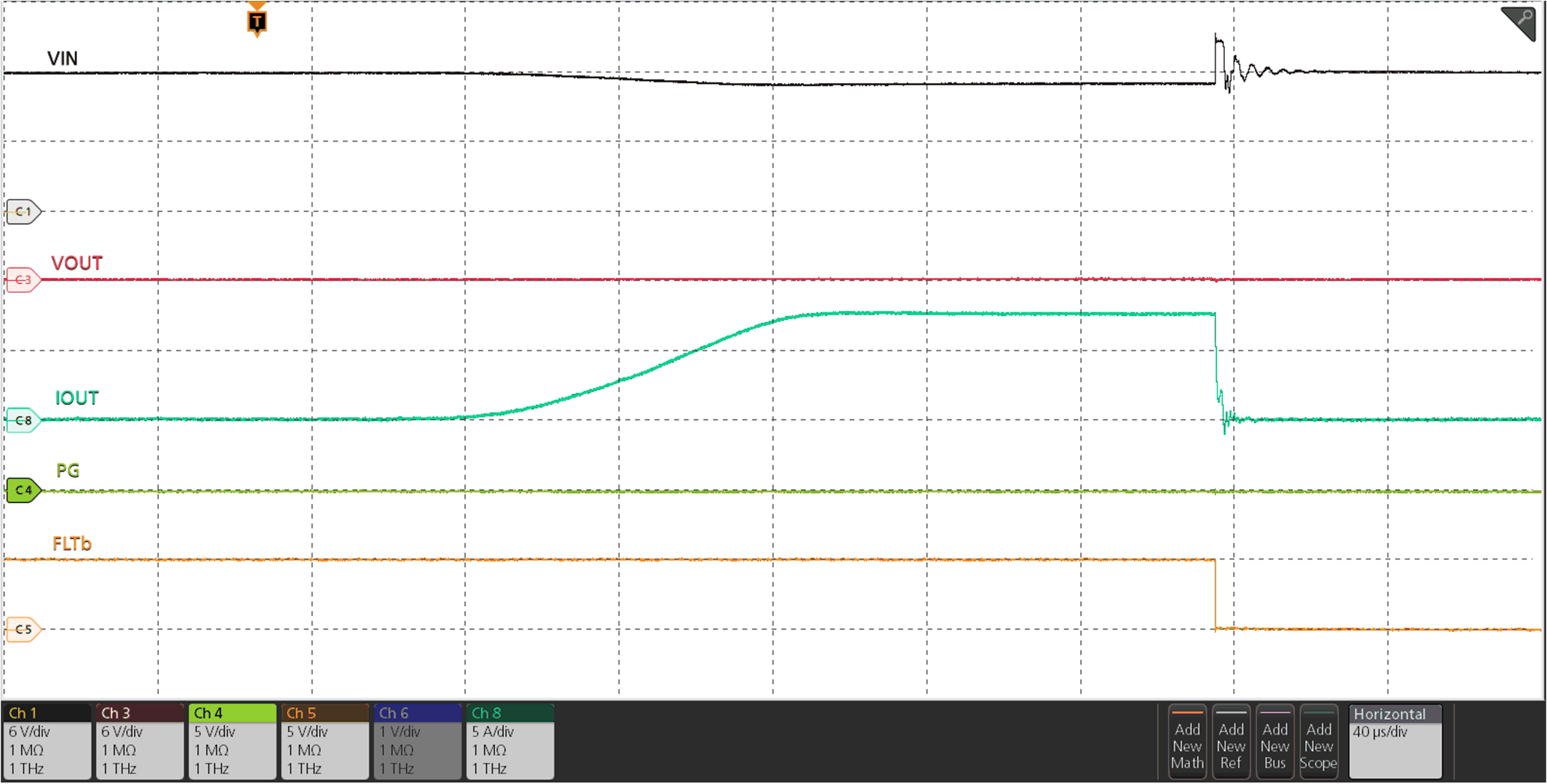
| VIN = 12 V, COUT = Open, OUT short circuit to GND, RIMON = 649 Ω, VEN/UVLO stepped from 0 V to 3.3 V |