JAJSIG1 January   2020 TPS22919-Q1

ADVANCE INFORMATION for pre-production products; subject to change without notice.  

  1. 特長
  2. アプリケーション
  3. 概要
    1.     Device Images
      1.      概略回路図
  4. 改訂履歴
  5. 概要 (続き)
  6. Pin Configuration and Functions
    1.     Pin Functions
  7. Specifications
    1. 7.1 Absolute Maximum Ratings
    2. 7.2 ESD Ratings
    3. 7.3 Recommended Operating Conditions
    4. 7.4 Thermal Information
    5. 7.5 Electrical Characteristics
    6. 7.6 Switching Characteristics
    7. 7.7 Typical Characteristics
  8. Parameter Measurement Information
    1. 8.1 Test Circuit and Timing Waveforms Diagrams
  9. Detailed Description
    1. 9.1 Overview
    2. 9.2 Functional Block Diagram
    3. 9.3 Feature Description
      1. 9.3.1 On and Off Control
      2. 9.3.2 Output Short Circuit Protection (ISC)
      3. 9.3.3 Fall Time (tFALL) and Quick Output Discharge (QOD)
        1. 9.3.3.1 QOD When System Power is Removed
    4. 9.4 Device Functional Modes
  10. 10Application and Implementation
    1. 10.1 Application Information
    2. 10.2 Typical Application
      1. 10.2.1 Design Requirements
      2. 10.2.2 Detailed Design Procedure
        1. 10.2.2.1 Limiting Inrush Current
        2. 10.2.2.2 Setting Fall Time for Shutdown Power Sequencing
        3. 10.2.2.3 Application Curves
  11. 11Power Supply Recommendations
  12. 12Layout
    1. 12.1 Layout Guidelines
    2. 12.2 Layout Example
    3. 12.3 Thermal Considerations
  13. 13デバイスおよびドキュメントのサポート
    1. 13.1 商標
    2. 13.2 静電気放電に関する注意事項
    3. 13.3 Glossary
  14. 14メカニカル、パッケージ、および注文情報

パッケージ・オプション

メカニカル・データ(パッケージ|ピン)
サーマルパッド・メカニカル・データ
発注情報

Output Short Circuit Protection (ISC)

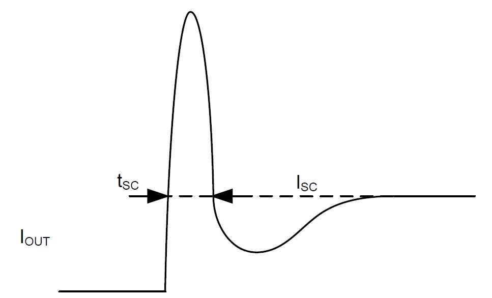
The device will limit current to the output in case of output shorts. When a short occurs, the large VIN to VOUT voltage drop causes the switch to limit the output current (ISC) within (tSC). When the output is below the hard short threshold (VSC), a lower limit is used to minimize the power dissipation while the fault is present. The device will continue to limit the current until it reaches its thermal shutdown temperature. At this time, the device will turn off until its temperature has lowered by the thermal hysteresis (35°C typical) before turning on again.
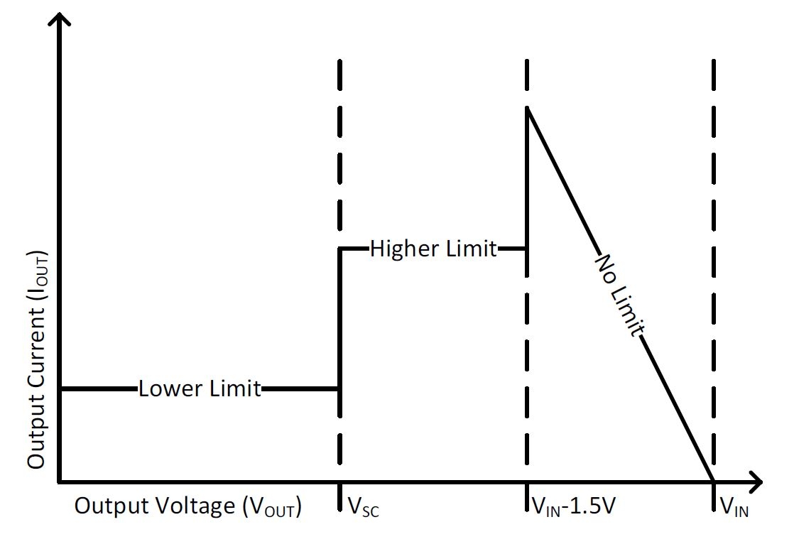
TPS22919-Q1 SCP1.jpgFigure 28. Output Short Circuit Current Limit
TPS22919-Q1 SCP2.jpgFigure 29. Output Short Circuit Response