JAJSIG1 January   2020 TPS22919-Q1

ADVANCE INFORMATION for pre-production products; subject to change without notice.  

  1. 特長
  2. アプリケーション
  3. 概要
    1.     Device Images
      1.      概略回路図
  4. 改訂履歴
  5. 概要 (続き)
  6. Pin Configuration and Functions
    1.     Pin Functions
  7. Specifications
    1. 7.1 Absolute Maximum Ratings
    2. 7.2 ESD Ratings
    3. 7.3 Recommended Operating Conditions
    4. 7.4 Thermal Information
    5. 7.5 Electrical Characteristics
    6. 7.6 Switching Characteristics
    7. 7.7 Typical Characteristics
  8. Parameter Measurement Information
    1. 8.1 Test Circuit and Timing Waveforms Diagrams
  9. Detailed Description
    1. 9.1 Overview
    2. 9.2 Functional Block Diagram
    3. 9.3 Feature Description
      1. 9.3.1 On and Off Control
      2. 9.3.2 Output Short Circuit Protection (ISC)
      3. 9.3.3 Fall Time (tFALL) and Quick Output Discharge (QOD)
        1. 9.3.3.1 QOD When System Power is Removed
    4. 9.4 Device Functional Modes
  10. 10Application and Implementation
    1. 10.1 Application Information
    2. 10.2 Typical Application
      1. 10.2.1 Design Requirements
      2. 10.2.2 Detailed Design Procedure
        1. 10.2.2.1 Limiting Inrush Current
        2. 10.2.2.2 Setting Fall Time for Shutdown Power Sequencing
        3. 10.2.2.3 Application Curves
  11. 11Power Supply Recommendations
  12. 12Layout
    1. 12.1 Layout Guidelines
    2. 12.2 Layout Example
    3. 12.3 Thermal Considerations
  13. 13デバイスおよびドキュメントのサポート
    1. 13.1 商標
    2. 13.2 静電気放電に関する注意事項
    3. 13.3 Glossary
  14. 14メカニカル、パッケージ、および注文情報

パッケージ・オプション

メカニカル・データ(パッケージ|ピン)
サーマルパッド・メカニカル・データ
発注情報

Pin Configuration and Functions

DCK Package
6-Pin SC-70
Top View
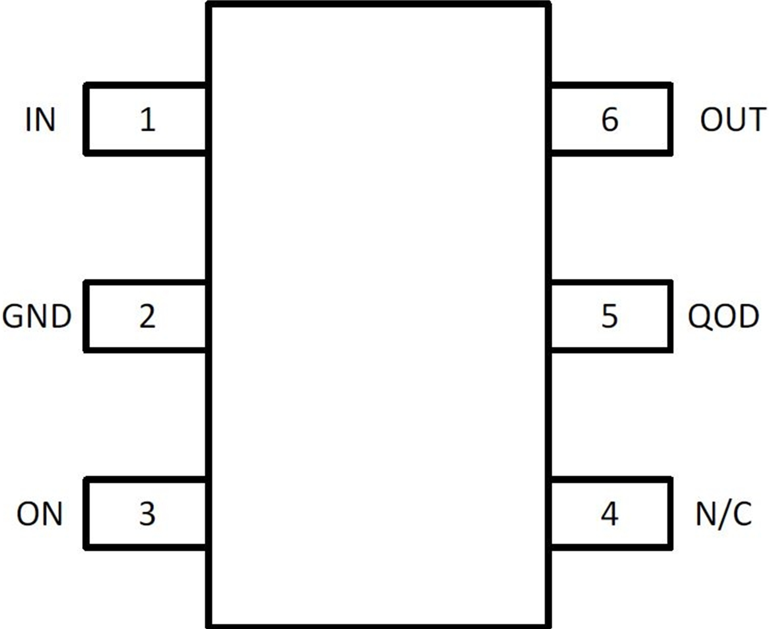
TPS22919-Q1 Pinout.png

Pin Functions

PIN I/O DESCRIPTION
NO. NAME
1 IN I Switch input.
2 GND Device ground.
3 ON I Active high switch control input. Do not leave floating.
4 NC No connect pin, leave floating.
5 QOD O Quick Output Discharge pin. This functionality can be enabled in one of three ways.
  • Placing an external resistor between VOUT and QOD
  • Tying QOD directly to VOUT and using the internal resistor value (RPD)
  • Disabling QOD by leaving pin floating
See the Fall Time (tFALL) and Quick Output Discharge (QOD) section for more information.
6 VOUT O Switch output.