SLVS840D November   2015  – August 2016 TPS22925

PRODUCTION DATA.  

  1. Features
  2. Applications
  3. Description
  4. Revision History
  5. Device Comparison Table
  6. Pin Configuration and Functions
  7. Specifications
    1. 7.1 Absolute Maximum Ratings
    2. 7.2 ESD Ratings
    3. 7.3 Recommended Operating Conditions
    4. 7.4 Thermal Information
    5. 7.5 Electrical Characteristics
    6. 7.6 Switching Characteristics
    7. 7.7 Typical Characteristics
    8. 7.8 Typical Characteristics
  8. Detailed Description
    1. 8.1 Overview
    2. 8.2 Functional Block Diagram
    3. 8.3 Feature Description
      1. 8.3.1 ON and OFF Control
      2. 8.3.2 Quick Output Discharge (QOD) (TPS22925B and TPS22925C Only)
      3. 8.3.3 Reverse Current Blocking
    4. 8.4 Device Functional Modes
  9. Application and Implementation
    1. 9.1 Application Information
      1. 9.1.1 VIN to VOUT Voltage Drop
      2. 9.1.2 Input Capacitor (CIN)
      3. 9.1.3 Load Capacitor (CL)
      4. 9.1.4 Standby Power Reduction
      5. 9.1.5 Power Multiplexing
      6. 9.1.6 Thermal Considerations
    2. 9.2 Typical Application
      1. 9.2.1 Design Requirements
      2. 9.2.2 Detailed Design Procedure
        1. 9.2.2.1 Managing Inrush Current
      3. 9.2.3 Application Curve
  10. 10Power Supply Recommendations
  11. 11Layout
    1. 11.1 Layout Guidelines
    2. 11.2 Layout Example
  12. 12Device and Documentation Support
    1. 12.1 Documentation Support
      1. 12.1.1 Related Documentation
    2. 12.2 Receiving Notification of Documentation Updates
    3. 12.3 Community Resources
    4. 12.4 Trademarks
    5. 12.5 Electrostatic Discharge Caution
    6. 12.6 Glossary
  13. 13Mechanical, Packaging, and Orderable Information

パッケージ・オプション

メカニカル・データ(パッケージ|ピン)
サーマルパッド・メカニカル・データ
発注情報

6 Pin Configuration and Functions

YPH Package
6-Pin DSBGA
Top View
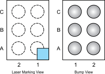
TPS22925 po_slvs840.gif

Pin Assignments

C GND ON
B VOUT VIN
A VOUT VIN
1 2

Pin Functions

PIN TYPE DESCRIPTION
NAME NO.
GND C1 GND Ground
ON C2 I Switch control input. Active high. Do not leave floating.
VIN A2 I Switch input; bypass this input with a ceramic capacitor to ground. See the Application Information section for more detail.
B2
VOUT A1 O Switch output
B1