JAJSN24A November 2021 – June 2022 TPS22953-Q1 , TPS22954-Q1
PRODUCTION DATA
- 1 特長
- 2 アプリケーション
- 3 概要
- 4 Revision History
- 5 Device Comparison Table
- 6 Pin Configuration and Functions
-
7 Specifications
- 7.1 Absolute Maximum Ratings
- 7.2 ESD Ratings
- Recommended Operating Conditions
- 7.3 Thermal Information
- 7.4 Electrical Characteristics
- 7.5 Electrical Characteristics – VBIAS = 5 V
- 7.6 Electrical Characteristics – VBIAS = 3.3 V
- 7.7 Electrical Characteristics – VBIAS = 2.5 V
- 7.8 Switching Characteristics – CT = 1000 pF
- 7.9 Switching Characteristics – CT = 0 pF
- 7.10 Typical DC Characteristics
- 7.11 Typical Switching Characteristics
- 8 Parameter Measurement Information
-
9 Detailed Description
- 9.1 Overview
- 9.2 Functional Block Diagram
- 9.3
Feature Description
- 9.3.1 On and Off Control (EN Pin)
- 9.3.2 Voltage Monitoring (SNS Pin)
- 9.3.3 Power Good (PG Pin)
- 9.3.4 Supervisor Fault Detection and Automatic Restart
- 9.3.5 Manual Restart
- 9.3.6 Thermal Shutdown
- 9.3.7 Reverse Current Blocking (TPS22953-Q1 Only)
- 9.3.8 Quick Output Discharge (QOD) (TPS22954-Q1 Only)
- 9.3.9 VIN and VBIAS Voltage Range
- 9.3.10 Adjustable Rise Time (CT Pin)
- 9.3.11 Power Sequencing
- 9.4 Device Functional Modes
- 10Application and Implementation
- 11Power Supply Recommendations
- 12Layout
- 13Device and Documentation Support
- 14Mechanical, Packaging, and Orderable Information
パッケージ・オプション
メカニカル・データ(パッケージ|ピン)
- DQC|10
サーマルパッド・メカニカル・データ
- DQC|10
発注情報
10.1.7 Make-Before-Break Power MUX (TPS22953-Q1 Only)
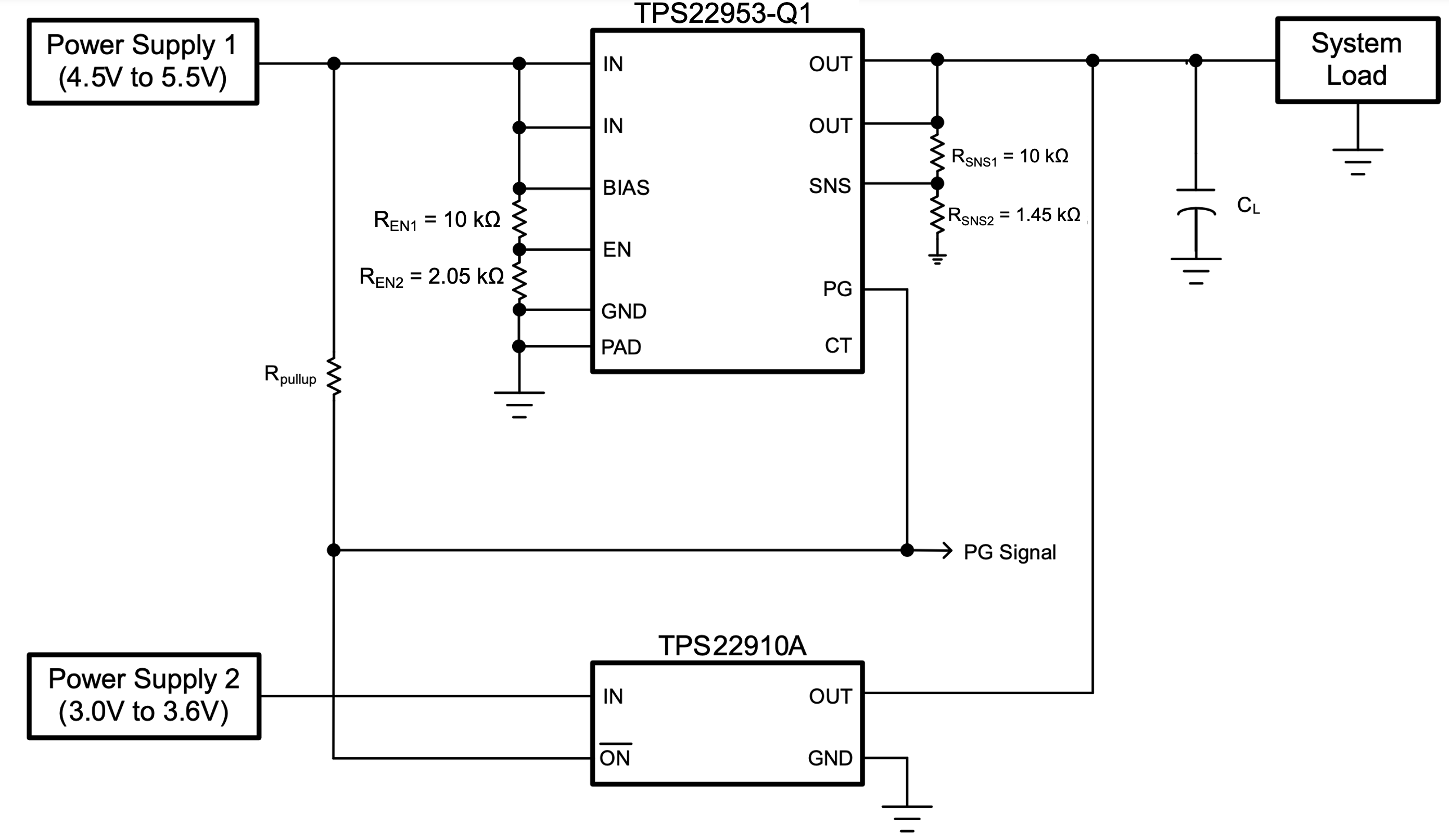
The reverse current blocking feature of the TPS22953-Q1 makes it suitable for power multiplexing (MUXing) between two power supplies with different voltages. The SNS and PG pin can be configured to implement make-before-break logic. The circuit in Figure 10-5 shows how the detection of Load Switch 1 turning on can be used to disable the load switch for power supply 2. By tying SNS to the Load, the PG is pulled up when the output voltage starts to rise. This event disables an active low load switch such as the TPS22910A.
 Figure 10-5 Make-Before-Break Power MUX Schematic
The make-before-break logic ensures that power supply 2 is not disconnected until power supply 1 is connected. Unlike break-before-make logic, this approach is ideal for preventing voltage dip on the output when switching between supplies. However, in most cases, this approach also results in temporary reverse current flow.
The TPS22910A is well suited for this application because it can detect and block reverse current even before it is disabled by the TPS22953-Q1 PG signal. Also, the active low enable of the TPS22910A eliminates the need for an inverter as shown in the previous example.
To ensure correct logic, the SNS pin must be configured to toggle PG when the load voltage is between the two supply voltages (3.6 V to 4.5 V). The SNS resistor values in Figure 10-5 are assuming a tolerance of ±1% or better.
Table 10-2 summarizes the logic of the PG Signal for Figure 10-5.
| PG Signal | Indication |
|---|---|
| H | Power supply 1 present. System powered from power supply 1. |
| L | Power supply 1 not present. System powered from power supply 2. |