JAJSN24A November 2021 – June 2022 TPS22953-Q1 , TPS22954-Q1
PRODUCTION DATA
- 1 特長
- 2 アプリケーション
- 3 概要
- 4 Revision History
- 5 Device Comparison Table
- 6 Pin Configuration and Functions
-
7 Specifications
- 7.1 Absolute Maximum Ratings
- 7.2 ESD Ratings
- Recommended Operating Conditions
- 7.3 Thermal Information
- 7.4 Electrical Characteristics
- 7.5 Electrical Characteristics – VBIAS = 5 V
- 7.6 Electrical Characteristics – VBIAS = 3.3 V
- 7.7 Electrical Characteristics – VBIAS = 2.5 V
- 7.8 Switching Characteristics – CT = 1000 pF
- 7.9 Switching Characteristics – CT = 0 pF
- 7.10 Typical DC Characteristics
- 7.11 Typical Switching Characteristics
- 8 Parameter Measurement Information
-
9 Detailed Description
- 9.1 Overview
- 9.2 Functional Block Diagram
- 9.3
Feature Description
- 9.3.1 On and Off Control (EN Pin)
- 9.3.2 Voltage Monitoring (SNS Pin)
- 9.3.3 Power Good (PG Pin)
- 9.3.4 Supervisor Fault Detection and Automatic Restart
- 9.3.5 Manual Restart
- 9.3.6 Thermal Shutdown
- 9.3.7 Reverse Current Blocking (TPS22953-Q1 Only)
- 9.3.8 Quick Output Discharge (QOD) (TPS22954-Q1 Only)
- 9.3.9 VIN and VBIAS Voltage Range
- 9.3.10 Adjustable Rise Time (CT Pin)
- 9.3.11 Power Sequencing
- 9.4 Device Functional Modes
- 10Application and Implementation
- 11Power Supply Recommendations
- 12Layout
- 13Device and Documentation Support
- 14Mechanical, Packaging, and Orderable Information
パッケージ・オプション
メカニカル・データ(パッケージ|ピン)
- DQC|10
サーマルパッド・メカニカル・データ
- DQC|10
発注情報
6 Pin Configuration and Functions
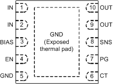
 Figure 6-1 DQC/DSQ Package10-Pin WSONTop View
 Figure 6-2 DQC/DSQ Package10-Pin WSONBottom View
Table 6-1 Pin Functions
| PIN(1) | I/O | DESCRIPTION | |
|---|---|---|---|
| NO. | NAME | ||
| 1 | IN | I | Switch input. Bypass this input with a ceramic capacitor to GND. |
| 2 | |||
| 3 | BIAS | I | Bias pin and power supply to the device |
| 4 | EN | I | Active high switch to enable and disable the output. Also acts as the input UVLO pin. Use external resistor divider to adjust the UVLO level. Do not leave floating. |
| 5 | GND | — | Device ground |
| 6 | CT | O | VOUT slew rate control. Place ceramic cap from CT to GND to change the VOUT slew rate of the device and limit the inrush current. Rate the CT Capacitor to 25 V or higher. |
| 7 | PG | O | Power Good. This pin is open drain which pulls low when the voltage on EN or SNS is below their respective VIL levels. |
| 8 | SNS | I | Sense pin. Use external resistor divider to adjust the power good level. Do not leave floating. |
| 9 | OUT | O | Switch output |
| 10 | |||
| — | Thermal Pad | — | Exposed thermal pad. Tie to GND. |
(1) Pinout applies to all package versions.