SLVSCX7A February 2015 – March 2015 TPS22958
PRODUCTION DATA.
- 1 Features
- 2 Applications
- 3 Description
- 4 Revision History
- 5 Device Comparison Table
- 6 Pin Configuration and Functions
-
7 Specifications
- 7.1 Absolute Maximum Ratings
- 7.2 ESD Ratings
- 7.3 Recommended Operating Conditions
- 7.4 Thermal Information
- 7.5 Electrical Characteristics (VBIAS = 5 V)
- 7.6 Electrical Characteristics (VBIAS = 3.3 V)
- 7.7 Electrical Characteristics (VBIAS = 2.5 V)
- 7.8 Switching Characteristics
- 7.9 Typical DC Characteristics
- 7.10 Typical AC Characteristics
- 8 Parameter Measurement Information
- 9 Detailed Description
- 10Application and Implementation
- 11Power Supply Recommendations
- 12Layout
- 13Device and Documentation Support
- 14Mechanical, Packaging, and Orderable Information
パッケージ・オプション
メカニカル・データ(パッケージ|ピン)
サーマルパッド・メカニカル・データ
- DGN|8
発注情報
9 Detailed Description
9.1 Overview
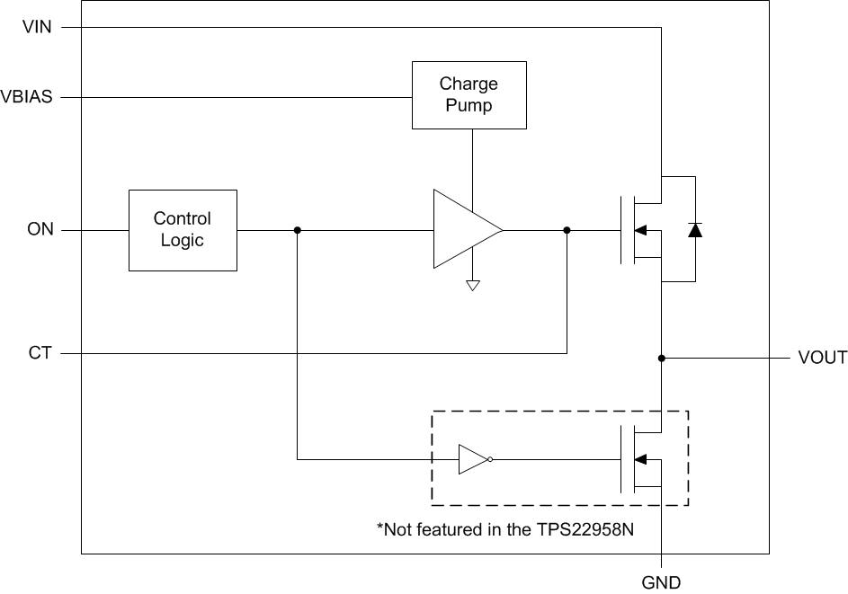
This device is a 5.5 V, 4 A / 6 A, single channel load switch with an adjustable rise time. The device contains an N-channel MOSFET controlled by an on/off GPIO-compatible input. The ON pin must be connected and cannot be left floating. The device is designed to control the turn-on rate and therefore the inrush current. By controlling the inrush current, power supply sag can be reduced during turn on. The slew rate is set by connecting a capacitor from the CT pin to GND.
The slew rate is proportional to the capacitor on the CT pin. Refer to the Adjustable Rise Time section to determine the correct CT value for a desired rise time.
The internal circuitry is powered by the VBIAS pin, which supports voltages from 2.5 to 5.5 V. This circuitry includes the charge pump, QOD, and control logic. For these internal blocks to function correctly, a voltage between 2.5 and 5.5 V must be supplied to VBIAS.
When a voltage is supplied to VBIAS and the ON pin goes low, the QOD turns on. This connects VOUT to GND through an on-chip resistor and is not a feature for the TPS22958N. The typical pull-down resistance (RPD) is 135 Ω.
9.2 Functional Block Diagram

9.3 Feature Description
9.3.1 ON/OFF Control
The ON pin controls the state of the switch. Asserting ON high enables the switch. ON is active high and has a low threshold, making it capable of interfacing with low-voltage signals. The ON pin is compatible with standard GPIO logic threshold. It can be used with any microcontroller with 1.2 V or higher GPIO voltage. This pin cannot be left floating and must be tied either high or low for proper functionality.
9.3.2 Quick Output Discharge (QOD)
The TPS22958 includes a QOD feature while the TPS22958N does not. When the device is disabled, a discharge resistor is connected between VOUT and GND. This resistor has a typical value of 135 Ω and prevents the output from floating while the switch is disabled.
9.3.3 VIN and VBIAS Voltage Range
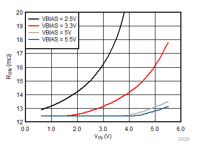
For optimal RON performance, make sure VIN ≤ VBIAS. The device will still function if VIN > VBIAS but will exhibit an RON greater than what is listed in the Electrical Characteristics table. See Figure 35 for an example of a typical device. RON increases as VIN exceeds the VBIAS voltage. For the maximum voltage ratings on the VIN and VBIAS pins, please refer to the Absolute Maximum Ratings table.

| TA = 25°C | IOUT = -200 mA | VON = 5 V | ||
9.3.4 Adjustable Rise Time
A capacitor from the CT pin to GND sets the slew rate, and it should be rated for 25 V and above. An approximate formula for the relationship between CT and slew rate with VBIAS = 5 V is:
where
- SR = slew rate (in µs/V)
- CT = the capacitance value on the CT pin (in pF)
- The units for the constant 14.78 is µs/V.
- The units for the constant 0.146 is µs/(V×pF)
Rise time can be calculated by multiplying the input voltage by the slew rate. Table 1 contains rise time values measured on a typical device.
Table 1. Rise Time Table
| CTx (pF) | RISE TIME (µs) 10% - 90%, CL = 0.1 µF, CIN = 1 µF, RL = 10 Ω, VBIAS = 5 V
Typical values at 25°C with a 25-V X7R 10% ceramic capacitor on CT |
||||||
|---|---|---|---|---|---|---|---|
| VIN = 5 V | VIN = 3.3 V | VIN = 1.8 V | VIN = 1.5 V | VIN = 1.2 V | VIN = 0.8 V | VIN = 0.6 V | |
| 0 | 79 | 59 | 41 | 37 | 33 | 26 | 23 |
| 220 | 227 | 158 | 97 | 86 | 74 | 55 | 48 |
| 470 | 397 | 270 | 160 | 139 | 116 | 88 | 72 |
| 1000 | 769 | 522 | 301 | 258 | 211 | 153 | 126 |
| 2200 | 1659 | 1118 | 640 | 548 | 450 | 315 | 256 |
| 4700 | 3445 | 2314 | 1315 | 1128 | 927 | 656 | 528 |
| 10000 | 7310 | 4884 | 2778 | 2372 | 1950 | 1379 | 1103 |
9.4 Device Functional Modes
The following table lists the VOUT pin connections for a particular device as determined by the ON pin.
Table 2. VOUT Functional Table
| ON (Control Input) | TPS22958 | TPS22958N |
|---|---|---|
| L | GND | Open |
| H | VIN | VIN |