SLVSCX7A February 2015 – March 2015 TPS22958
PRODUCTION DATA.
- 1 Features
- 2 Applications
- 3 Description
- 4 Revision History
- 5 Device Comparison Table
- 6 Pin Configuration and Functions
-
7 Specifications
- 7.1 Absolute Maximum Ratings
- 7.2 ESD Ratings
- 7.3 Recommended Operating Conditions
- 7.4 Thermal Information
- 7.5 Electrical Characteristics (VBIAS = 5 V)
- 7.6 Electrical Characteristics (VBIAS = 3.3 V)
- 7.7 Electrical Characteristics (VBIAS = 2.5 V)
- 7.8 Switching Characteristics
- 7.9 Typical DC Characteristics
- 7.10 Typical AC Characteristics
- 8 Parameter Measurement Information
- 9 Detailed Description
- 10Application and Implementation
- 11Power Supply Recommendations
- 12Layout
- 13Device and Documentation Support
- 14Mechanical, Packaging, and Orderable Information
パッケージ・オプション
メカニカル・データ(パッケージ|ピン)
サーマルパッド・メカニカル・データ
- DGN|8
発注情報
12 Layout
12.1 Layout Guidelines
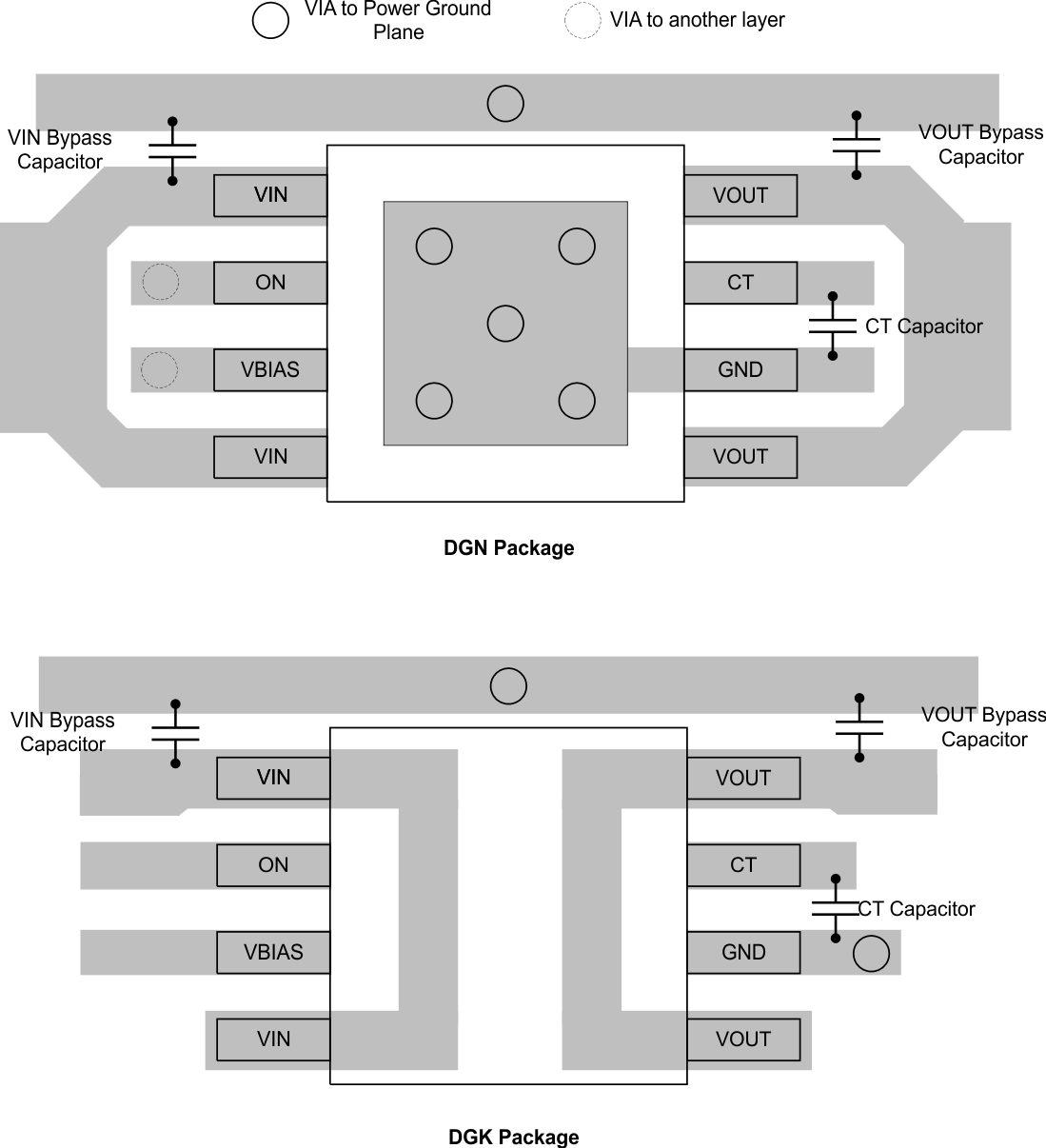
- VIN and VOUT traces should be as short and wide as possible to accommodate for high current. When connecting the two VIN or VOUT pins together, an equal trace length should be used to avoid an unequal distribution of current through each pin.
- Use vias under the exposed thermal pad to connect to the power ground plane for thermal relief during high current operation.
- VIN pins should be bypassed to ground with low-ESR ceramic bypass capacitors. The typical recommended bypass capacitance is 1-µF ceramic with X5R or X7R dielectric. This capacitor should be placed as close to the device pins as possible.
- VOUT pins should be bypassed to ground with low-ESR ceramic bypass capacitors. The typical recommended bypass capacitance is one-tenth of the VIN bypass capacitor of X5R or X7R dielectric rating. This capacitor should be placed as close to the device pins as possible.
- The CT capacitor should be placed as close to the device pins as possible. The typical recommended CT capacitance is a capacitor of X5R or X7R dielectric rating with a rating of 25 V or higher.
12.2 Layout Example
