JAJSDN1B April   2017  – December 2017 TPS22971

PRODUCTION DATA.  

  1. 特長
  2. アプリケーション
  3. 概要
  4. 改訂履歴
  5. Pin Configuration and Functions
  6. Specifications
    1. 6.1 Absolute Maximum Ratings
    2. 6.2 ESD Ratings
    3. 6.3 Recommended Operating Conditions
    4. 6.4 Thermal Information
    5. 6.5 Electrical Characteristics
    6. 6.6 Switching Characteristics
    7. 6.7 Typical DC Characteristics
    8. 6.8 Typical AC Characteristics
  7. Parameter Measurement Information
  8. Detailed Description
    1. 8.1 Overview
    2. 8.2 Functional Block Diagram
    3. 8.3 Feature Description
      1. 8.3.1 On and Off Control
      2. 8.3.2 Controlled Turn-On
      3. 8.3.3 Power Good (PG)
      4. 8.3.4 Quick Output Discharge (QOD)
    4. 8.4 Device Functional Modes
  9. Application and Implementation
    1. 9.1 Application Information
      1. 9.1.1 Thermal Consideration
      2. 9.1.2 PG Pull Up Resistor
      3. 9.1.3 Power Sequencing
    2. 9.2 Typical Application
      1. 9.2.1 Design Requirements
      2. 9.2.2 Detailed Design Procedure
        1. 9.2.2.1 Maximum Voltage Drop and On-Resistance
        2. 9.2.2.2 Managing Inrush Current
      3. 9.2.3 Application Curves
  10. 10Power Supply Recommendations
  11. 11Layout
    1. 11.1 Layout Guidelines
    2. 11.2 Layout Example
  12. 12デバイスおよびドキュメントのサポート
    1. 12.1 ドキュメントのサポート
      1. 12.1.1 関連資料
    2. 12.2 ドキュメントの更新通知を受け取る方法
    3. 12.3 コミュニティ・リソース
    4. 12.4 商標
    5. 12.5 静電気放電に関する注意事項
    6. 12.6 Glossary
  13. 13メカニカル、パッケージ、および注文情報

パッケージ・オプション

メカニカル・データ(パッケージ|ピン)
サーマルパッド・メカニカル・データ
発注情報

Layout

Layout Guidelines

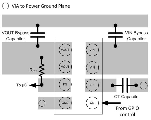
All traces must be as short as possible for best performance. Using wide traces for VIN, VOUT, and GND helps minimize the parasitic electrical effects along with minimizing the thermal impedance. The CT trace must be as short as possible to reduce parasitic capacitance.

Layout Example

TPS22971 Layout.jpg Figure 30. Package Layout Examples