JAJSEO7I October 2008 – December 2017 TPS23754 , TPS23754-1 , TPS23756
PRODUCTION DATA.
- 1 特長
- 2 アプリケーション
- 3 概要
- 4 改訂履歴
- 5 概要(続き)
- 6 Pin Configuration and Functions
- 7 Specifications
-
8 Detailed Description
- 8.1 Overview
- 8.2 Functional Block Diagram
- 8.3 Feature Description
- 8.4
Device Functional Modes
- 8.4.1
PoE Overview
- 8.4.1.1 Threshold Voltages
- 8.4.1.2 PoE Start-Up Sequence
- 8.4.1.3 Detection
- 8.4.1.4 Hardware Classification
- 8.4.1.5 Inrush and Start-Up
- 8.4.1.6 Maintain Power Signature
- 8.4.1.7 Start-Up and Converter Operation
- 8.4.1.8 PD Hotswap Operation
- 8.4.1.9 Converter Controller Features
- 8.4.1.10 Bootstrap Topology
- 8.4.1.11 Current Slope Compensation and Current Limit
- 8.4.1.12 Blanking – RBLNK
- 8.4.1.13 Dead Time
- 8.4.1.14 FRS and Synchronization
- 8.4.1.15 T2P, Start-Up, and Power Management
- 8.4.1.16 Thermal Shutdown
- 8.4.1.17 Adapter ORing
- 8.4.1.18 PPD ORing Features
- 8.4.1.19 Using DEN to Disable PoE
- 8.4.1.20 ORing Challenges
- 8.4.1
PoE Overview
-
9 Application and Implementation
- 9.1 Application Information
- 9.2
Typical Application
- 9.2.1 Design Requirements
- 9.2.2
Detailed Design Procedure
- 9.2.2.1 Input Bridges and Schottky Diodes
- 9.2.2.2 Protection, D1
- 9.2.2.3 Capacitor, C1
- 9.2.2.4 Detection Resistor, RDEN
- 9.2.2.5 Classification Resistor, RCLS
- 9.2.2.6 Dead Time Resistor, RDT
- 9.2.2.7 Switching Transformer Considerations and RVC
- 9.2.2.8 Special Switching MOSFET Considerations
- 9.2.2.9 Thermal Considerations and OTSD
- 9.2.2.10 APD Pin Divider Network, RAPD1, RAPD2
- 9.2.2.11 PPD Pin Divider Network, RPPD1, RPPD2
- 9.2.2.12 Setting Frequency (RFRS) and Synchronization
- 9.2.2.13 Current Slope Compensation
- 9.2.2.14 Blanking Period, RBLNK
- 9.2.2.15 Estimating Bias Supply Requirements and CVC
- 9.2.2.16 T2P Pin Interface
- 9.2.2.17 Advanced ORing Techniques
- 9.2.2.18 Soft Start
- 9.2.2.19 Frequency Dithering for Conducted Emissions Control
- 9.2.3 Application Curves
- 10Power Supply Recommendations
- 11Layout
- 12デバイスおよびドキュメントのサポート
- 13メカニカル、パッケージ、および注文情報
パッケージ・オプション
デバイスごとのパッケージ図は、PDF版データシートをご参照ください。
メカニカル・データ(パッケージ|ピン)
- PWP|20
サーマルパッド・メカニカル・データ
- PWP|20
発注情報
8.4.1.8 PD Hotswap Operation
IEEE 802.3at has taken a new approach to PSE output limiting. A type 2 PSE must meet an output current versus time template with specified minimum and maximum sourcing boundaries. The peak output current may be as high as 50 A for 10 μs or 1.75 A for 75 ms. This makes robust protection of the PD device even more important than it was in IEEE 802.3-2008.
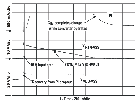
The internal hotswap MOSFET is protected against output faults and input voltage steps with a current limit and deglitched (time-delay filtered) foldback. An overload on the pass MOSFET engages the current limit, with VRTN-VVSS rising as a result. If VRTN rises above about 12 V for longer than about 400 μs, the current limit reverts to the inrush value, and turns the converter off. The 400 μs deglitch feature prevents momentary transients from causing a PD reset, provided that recovery lies within the bounds of the hotswap and PSE protection. Figure 25 shows an example of recovery from a 16 V PSE rising voltage step. The hotswap MOSFET goes into current limit, overshooting to a relatively low current, recovers to about 950-mA full current limit, and charges the input capacitor while the converter continues to run. The MOSFET did not go into foldback because VRTN-VVSS was less than 12 V after the 400 μs deglitch.
 Figure 25. Response to PSE Step Voltage
The PD control has a thermal sensor that protects the internal hotswap MOSFET. Conditions like start-up or operation into a VDD to RTN short cause high power dissipation in the MOSFET. An overtemperature shutdown (OTSD) turns off the hotswap MOSFET and class regulator, which are restarted after the device cools. The hotswap MOSFET will be re-enabled with the inrush current limit when exiting from an overtemperature event.
Pulling DEN to VSS during powered operation causes the internal hotswap MOSFET to turn off. This feature allows a PD with Option three ORing per Figure 26 to achieve adapter priority. Take care with synchronous converter topologies that can deliver power in both directions.
The hotswap switch will be forced off under the following conditions:
- VAPD above VAPDEN (about 1.5 V)
- VDEN< VPD-DIS when VVDD– VVSS is in the operational range
- PD over-temperature
- (VVDD– VVSS) < PoE UVLO (about 30.5 V)