JAJSNM6F November 2004 – January 2022 TPS2384
PRODUCTION DATA
- 1 特長
- 2 アプリケーション
- 3 概要
- 4 Revision History
- 5 Pin Configuration and Functions
- 6 Specifications
- 7 Parameter Measurement Information
-
8 Detailed Description
- 8.1 Overview
- 8.2 Functional Block Diagrams
- 8.3 Feature Description
- 8.4
Device Functional Modes
- 8.4.1 Auto Mode
- 8.4.2 Auto Mode Functional Description
- 8.4.3 AM Faults and INTB Output
- 8.4.4 Over and Undervoltage Fault
- 8.4.5 Over Current or Current Limit Faults
- 8.4.6 Undercurrent Fault (DC Modulated Disconnect)
- 8.4.7 Power Management Mode (PMM)
- 8.4.8 PMM Discovery 1
- 8.4.9 PMM Discovery 2
- 8.4.10 PMM Classification
- 8.4.11 PMM Legacy
- 8.4.12 PMM Rup Pwr
- 8.4.13 PMM RDWN
- 8.5 Programming
- 8.6
Register Maps
- 8.6.1 Register/Port Addressing Map
- 8.6.2 Common Read, Register Select
- 8.6.3 Common Write, Register Select = 1111 (Test Register)
- 8.6.4 Common Control Write, Register Select = 0001
- 8.6.5 Port Control Write 1, Register Select = 0010 (One Per Port)
- 8.6.6 Port Control Write 2, Register Select = 0011 (One Per Port)
- 8.6.7 Port Status Read 1, Register Select = 0100 (One Per Port)
- 8.6.8 Port Status Read 2, Register Select = 0101 (One Per Port)
- 8.6.9
A/D Results Registers (Discovery Current, Voltage, Current and Temperature)
- 8.6.9.1 Discovery Current — Lower Bits, Register Select = 0110 (One Per Port)
- 8.6.9.2 Discovery Current — Upper Bits, Register Select = 0111 (One Per Port)
- 8.6.9.3 Voltage — Lower Bits, Register Select = 1000 (One Per Port)
- 8.6.9.4 Voltage — Upper Bits, Register Select = 1001 (One Per Port)
- 8.6.9.5 Current — Lower Bits, Register Select = 1010 (One Per Port)
- 8.6.9.6 Current — Upper Bits, Register Select = 1011 (One Per Port)
- 8.6.9.7 Temperature — Lower Bits, Register Select = 1100 (One Per Port)
- 8.6.9.8 Temperature — Upper Bits, Register Select = 1101 (One Per Port)
- 9 Application and Implementation
- 10Power Supply Recommendations
- 11Layout
- 12Device and Documentation Support
- 13Mechanical, Packaging, and Orderable Information
パッケージ・オプション
メカニカル・データ(パッケージ|ピン)
サーマルパッド・メカニカル・データ
発注情報
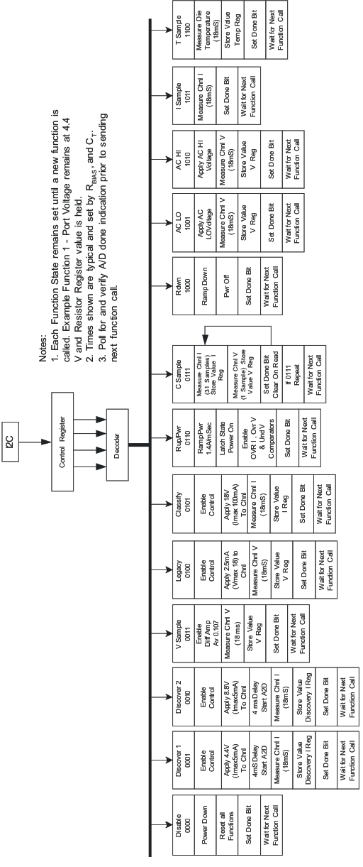
8.4.7.1 13 PMM Functions
- Disable: Disable the port and reset all functions.
- Discovery 1: Enable the Discovery 1 condition which applies a 4.4 V across the PD and measure and store the resulting current.
- Discovery 2: Enable the Discovery 2 condition which applies a 8.8 V across the PD and measure and store the resulting current.
- V Sample: Measure the voltage between the P and N pins and store the result in the A/D voltage register.
- Legacy: Enable the 3.5-mA current source for measuring capacitance and measure the voltage across the P and N terminals and store the result in the A/D voltage register.
- Classify: Enable the classification condition which applies 17.7 V across the PD and measure and store the resulting current.
- Rup Pwr: Turn on the output switch while controlling the current being delivered to the PD until the PD current needs are met or the max current is reached.
- C Sample: Continuous cycle of 31 current measurements and 1 voltage measurement. After each measurement the contents of the appropriate register are updated.
- Rdwn: Turn off the output switch while controlling current until output current reaches 0 mA.
- AC LO: Turns on low side output FET and measures voltage between P and N pin and store result in A/D voltage registers.
- AC HI: Turns on high side output FET and measures voltage between P and N pin and store result in A/D voltage registers.
- ISample: Measure the current and store the result in the A/D current register.
- TSample: Measure the internal die
temperature and store the result in the A/D temperature register.
Conversion times for A/D measurements performed as part of the functions listed above are generally as shown in the typical values in the Electrical Characteristics table. However, conversion time is somewhat dependant on the magnitude of the input signal being measured. Power management mode applications must take precautions to test the A/D DONE bit (MSB of the high byte) of the pertinent results register before accepting or using the returned value. A logic 1 at this bit location indicates the conversion is complete. Also, after an A/D conversion is in process on a given port, subsequent function calls to that port must wait until the currently executing conversion is complete. Commands written prior to completion can cause the results of the initial conversion to be written to the register of the subsequent function.
 Figure 8-11 Device Process Function Flow