JAJSNM6F November 2004 – January 2022 TPS2384
PRODUCTION DATA
- 1 特長
- 2 アプリケーション
- 3 概要
- 4 Revision History
- 5 Pin Configuration and Functions
- 6 Specifications
- 7 Parameter Measurement Information
-
8 Detailed Description
- 8.1 Overview
- 8.2 Functional Block Diagrams
- 8.3 Feature Description
- 8.4
Device Functional Modes
- 8.4.1 Auto Mode
- 8.4.2 Auto Mode Functional Description
- 8.4.3 AM Faults and INTB Output
- 8.4.4 Over and Undervoltage Fault
- 8.4.5 Over Current or Current Limit Faults
- 8.4.6 Undercurrent Fault (DC Modulated Disconnect)
- 8.4.7 Power Management Mode (PMM)
- 8.4.8 PMM Discovery 1
- 8.4.9 PMM Discovery 2
- 8.4.10 PMM Classification
- 8.4.11 PMM Legacy
- 8.4.12 PMM Rup Pwr
- 8.4.13 PMM RDWN
- 8.5 Programming
- 8.6
Register Maps
- 8.6.1 Register/Port Addressing Map
- 8.6.2 Common Read, Register Select
- 8.6.3 Common Write, Register Select = 1111 (Test Register)
- 8.6.4 Common Control Write, Register Select = 0001
- 8.6.5 Port Control Write 1, Register Select = 0010 (One Per Port)
- 8.6.6 Port Control Write 2, Register Select = 0011 (One Per Port)
- 8.6.7 Port Status Read 1, Register Select = 0100 (One Per Port)
- 8.6.8 Port Status Read 2, Register Select = 0101 (One Per Port)
- 8.6.9
A/D Results Registers (Discovery Current, Voltage, Current and Temperature)
- 8.6.9.1 Discovery Current — Lower Bits, Register Select = 0110 (One Per Port)
- 8.6.9.2 Discovery Current — Upper Bits, Register Select = 0111 (One Per Port)
- 8.6.9.3 Voltage — Lower Bits, Register Select = 1000 (One Per Port)
- 8.6.9.4 Voltage — Upper Bits, Register Select = 1001 (One Per Port)
- 8.6.9.5 Current — Lower Bits, Register Select = 1010 (One Per Port)
- 8.6.9.6 Current — Upper Bits, Register Select = 1011 (One Per Port)
- 8.6.9.7 Temperature — Lower Bits, Register Select = 1100 (One Per Port)
- 8.6.9.8 Temperature — Upper Bits, Register Select = 1101 (One Per Port)
- 9 Application and Implementation
- 10Power Supply Recommendations
- 11Layout
- 12Device and Documentation Support
- 13Mechanical, Packaging, and Orderable Information
パッケージ・オプション
メカニカル・データ(パッケージ|ピン)
サーマルパッド・メカニカル・データ
発注情報
8.4.11 PMM Legacy
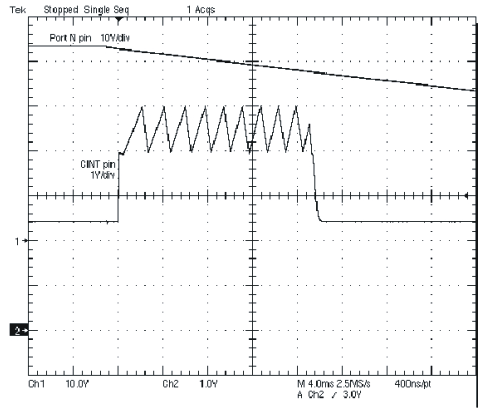
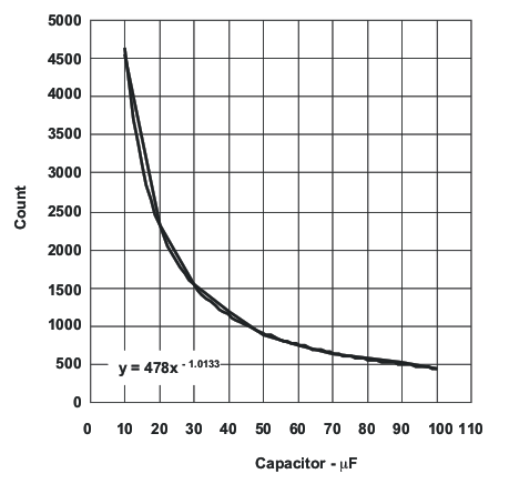
PMM Legacy function is used to detect PDs that are non compliant. Legacy detection uses a current source (typically 3.5 mA) as a test current while the A/D measures the average voltage for approximately 18 ms. The waveform shown in Figure 8-14 is the Legacy function charging a 10-μF capacitor. The capacitance charges to a value that is no greater than 20 V below the P port voltage. As the capacitor is charging the A/D is accumulating counts in the voltage A/D register. Figure 8-15 shows the relationship between port capacitance and the number of counts. A user can characterize non-compliant PD's signatures and use the Legacy function to recognize these devices.
 Figure 8-14 Legacy Detection Function Waveforms
 Figure 8-15 A/D Counts vs Legacy Port Capacitance