JAJS232E November 2006 – October 2019 TPS2410 , TPS2411
PRODUCTION DATA.
- 1 特長
- 2 アプリケーション
- 3 概要
- 4 改訂履歴
- 5 概要(続き)
- 6 Device Comparison
- 7 Pin Configuration and Functions
- 8 Specifications
- 9 Detailed Description
- 10Application and Implementation
- 11Power Supply Recommendations
- 12Layout
- 13デバイスおよびドキュメントのサポート
- 14メカニカル、パッケージ、および注文情報
10.2.3 ORing Examples
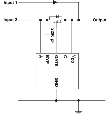
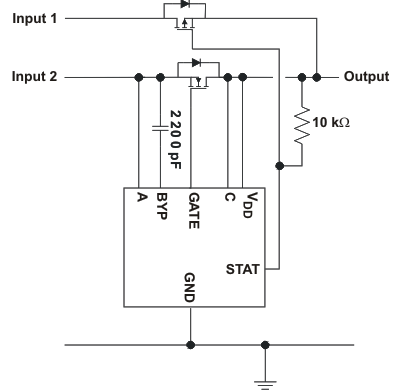
Applications with the TPS2410 and TPS2411 are not limited to ORIng of identical sections. The device and external MOSFET form a general purpose function block. Figure 14 shows a circuit with ORing between a discrete diode and a TPS2410 MOSFET section. This circuit can be used to combine two different voltages in cases where the output is re-regulated, and the additional voltage drop in the Input 1 path is not a concern. An example is ORing of an ac adapter on Input 1 with a lower voltage on Input 2 Figure 15 shows an improved efficiency version of the first in which a P MOSFET replaces the simple diode. This circuit may not be useful in applications where Input 1 may be shorted because the P MOSFET is not managed, permitting reverse current flow. Input 2 should be the lower of the two voltage rails. If Input 1 was the lower voltage rail and connected first, then Input 2 is connected, there is a momentary reverse current in the P MOSFET. The reverse current occurs because the STAT signal does not go high until VGATE ramps above Input 2 (the higher voltage) by 0.4 V. The Input 1 to Input 2 difference voltage momentarily appears across the PMOS device which is turned on until STAT switches high, causing a reverse current. The highest efficiency with the best fault tolerance is provided by two TPS2410 MOSFET sections.
 Figure 14. ORing Circuit
  Figure 15. P MOSFET Circuit
 The TPS2410 may be a better choice in applications where inputs may be removed, causing an open-circuit input. If the MOSFET was ON when the input is removed, VAC is virtually zero. If the reverse turn-off threshold is programmed negative, the device does not pull GATE low. A system interruption can then be created if a short is applied to the floating input. For example, if an ac adapter is first connected to the unit, and then connected to the ac mains, the adapter output capacitors look like a momentary short to the unit. A TPS2410 with RSET open turns the MOSFET OFF when the input goes open circuit.