SLVSAL2G January 2011 – November 2015 TPS24710 , TPS24711 , TPS24712 , TPS24713
PRODUCTION DATA.
- 1 Features
- 2 Applications
- 3 Description
- 4 Revision History
- 5 Device Comparison Table
- 6 Pin Configuration and Functions
- 7 Specifications
- 8 Detailed Description
-
9 Application and Implementation
- 9.1 Application Information
- 9.2
Typical Application
- 9.2.1 Design Requirements
- 9.2.2
Detailed Design Procedure
- 9.2.2.1
Power-Limited Start-Up
- 9.2.2.1.1 STEP 1. Choose RSENSE
- 9.2.2.1.2 STEP 2. Choose MOSFET M1
- 9.2.2.1.3 STEP 3. Choose Power-Limit Value, PLIM, and RPROG
- 9.2.2.1.4 STEP 4. Choose Output Voltage Rising Time, tON, CT
- 9.2.2.1.5 STEP 5. Calculate the Retry-Mode Duty Ratio
- 9.2.2.1.6 STEP 6. Select R1 and R2 for UV
- 9.2.2.1.7 STEP 7. Choose RGATE, R4, R5 and C1
- 9.2.2.2 Additional Design Considerations
- 9.2.2.1
Power-Limited Start-Up
- 9.2.3 Application Curve
- 10Power Supply Recommendations
- 11Layout
- 12Device and Documentation Support
- 13Mechanical, Packaging, and Orderable Information
9 Application and Implementation
NOTE
Information in the following applications sections is not part of the TI component specification, and TI does not warrant its accuracy or completeness. TI’s customers are responsible for determining suitability of components for their purposes. Customers should validate and test their design implementation to confirm system functionality.
9.1 Application Information
The TPS2471x is a hotswap used to manage inrush current and provide load fault protection. When designing a hotswap, three key scenarios should be considered:
- Start-up
- Output of a hotswap is shorted to ground when the hotswap is on. This is often referred to as a hot-short.
- Powering-up a board when the output and ground are shorted. This is usually called a start-into-short.
Each of these scenarios place stress on the hotswap MOSFET. Take special care when designing the hotswap circuit to keep the MOSFET within its SOA. The following design example is provided as a guide. Use the TPS24710 Design Calculator (SLVC566) to assist with the detailed design equation calculations.
9.2 Typical Application
This section provides an application example utilizing power limited start-up and MOSFET SOA protection. The design parameters are listed in the Design Requirements section and represent a more moderate level of fault current. For more stringent current levels, refer to either the TPS2471xEVM (SLUU459) (25 A design) or the calculator tool (SLVC566) (50 A design).
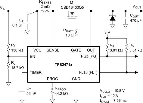 Figure 35. Typical Application (12 V at 10 A)
9.2.1 Design Requirements
For this design example, use the parameters shown in Table 1.
Table 1. Design Parameters
| PARAMETER | VALUE |
|---|---|
| Input voltage | 12 V ±2V |
| Maximum operating load current | 10 A |
| Operating temperature | 20°C —50°C |
| Fault trip current | 12 A |
| Load capacitance | 470 µF |
9.2.2 Detailed Design Procedure
9.2.2.1 Power-Limited Start-Up
This design example assumes a 12-V system voltage with an operating tolerance of ±2 V. The rated load current is 10 A, corresponding to a dc load of 1.2 Ω. If the current exceeds 12 A, then the controller should shut down and then attempt to restart. Ambient temperatures may range from 20°C to 50°C. The load has a minimum input capacitance of 470 μF. Figure 36 shows a simplified system block diagram of the proposed application.
This design procedure seeks to control the junction temperature of MOSFET M1 under both static and transient conditions by proper selection of package, cooling, rDS(on), current limit, fault timeout, and power limit. The design procedure further assumes that a unit running at full load and maximum ambient temperature experiences a brief input-power interruption sufficient to discharge COUT, but short enough to keep M1 from cooling. A full COUT recharge then takes place. Adjust this procedure to fit your application and design criteria.
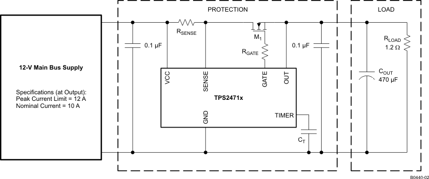 Figure 36. Simplified Block Diagram of the System Constructed in the Design Example
9.2.2.1.1 STEP 1. Choose RSENSE
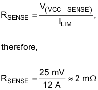
From the TPS24710/11/12/13 electrical specifications, the current-limit threshold voltage, V(VCC – SENSE), is around 25 mV. A resistance of 2 mΩ is selected for the peak current limit of 12 A, while dissipating only 200 mW at the rated 10-A current (see Equation 6). This represents a 0.17% power loss.
9.2.2.1.2 STEP 2. Choose MOSFET M1
The next design step is to select M1. The TPS24710/11/12/13 is designed to use an N-channel MOSFET with a gate-to-source voltage rating of 20 V.
Devices with lower gate-to-source voltage ratings can be used if a Zener diode is connected so as to limit the maximum gate-to-source voltage across the transistor.
The next factor to consider is the drain-to-source voltage rating, VDS(MAX), of the MOSFET. Although the MOSFET only sees 12 V DC, it may experience much higher transient voltages during extreme conditions, such as the abrupt shutoff that occurs during a fast trip. A TVS may be required to limit inductive transients under such conditions. A transistor with a VDS(MAX) rating of at least twice the nominal input power-supply voltage is recommended regardless of whether a TVS is used or not.
Next select the on resistance of the transistor, rDS(on). The maximum on-resistance must not generate a voltage greater then the minimum power-good threshold voltage of 140 mV. Assuming a current limit of 12 A, a maximum rDS(on) of 11.67 mΩ is required. Also consider the effect of rDS(on) upon the maximum operating temperature TJ(MAX) of the MOSFET. Equation 7 computes the value of rDS(on)(MAX) at a junction temperature of TJ(MAX). Most manufacturers list rDS(on)(MAX) at 25°C and provide a derating curve from which values at other temperatures can be derived. Compute the maximum allowable on-resistance, rDS(on)(MAX), using Equation 7.
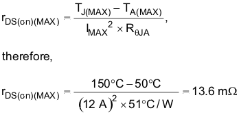
Taking these factors into consideration, the TI CSD16403Q5 was selected for this example. This transistor has a VGS(MAX) rating of 16 V, a VDS(MAX) rating of 25 V, and a maximum rDS(on) of 2.8 mΩ at room temperature. During normal circuit operation, the MOSFET can have up to 10 A flowing through it. The power dissipation of the MOSFET equates to 0.24 W and a 9.6°C rise in junction temperature. This is well within the data sheet limits for the MOSFET. The power dissipated during a fault (e.g., output short) is far larger than the steady-state power. The power handling capability of the MOSFET must be checked during fault conditions.
9.2.2.1.3 STEP 3. Choose Power-Limit Value, PLIM, and RPROG
MOSFET M1 dissipates large amounts of power during inrush. The power limit PLIM of the TPS24710/11/12/13 should be set to prevent the die temperature from exceeding a short-term maximum temperature, TJ(MAX)2. The short-term TJ(MAX)2 could be set as high as 130°C while still leaving ample margin to the usual manufacturer’s rating of 150°C. Equation 8 is an expression for calculating PLIM,

where RθJC is the junction-to-case thermal resistance of the MOSFET, rDS(on) is the resistance at the maximum operating temperature, and the factor of 0.8 represents the tolerance of the constant-power engine. For an ambient temperature of 50°C, the calculated maximum PLIM is 29.3 W. From Equation 2, a 44.2-kΩ, 1% resistor is selected for RPROG (see Equation 9).

VSNS-PL_MIN is the minimum sense voltage during power limit operation. Due to offsets of internal amplifiers, programmed power limit (PLIM) accuracy degrades at low VSNS-PL_MIN and could cause start-up issues. To ensure reliable operation, verify that VSNS,PL,MIN > 3 mV using Equation 10.

9.2.2.1.4 STEP 4. Choose Output Voltage Rising Time, tON, CT
The maximum output voltage rise time, tON, set by the timer capacitor CT must suffice to fully charge the load capacitance COUT without triggering the fault circuitry. Equation 11 defines tON for two possible inrush cases. Assuming that only the load capacitance draws current during start-up,
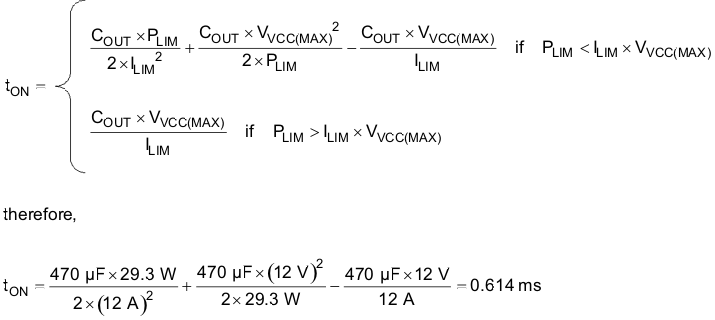
The next step is to determine the minimum fault-timer period. In Equation 11, the output rise time is tON. This is the amount of time it takes to charge the output capacitor up to the final output voltage. However, the fault timer uses the difference between the input voltage and the gate voltage to determine if the TPS24710/11/12/13 is still in inrush limit. The fault timer continues to run until VGS rises 5.9 V (for VVCC = 12 V) above the input voltage. Some additional time must be added to the charge time to account for this additional gate voltage rise. The minimum fault time can be calculated using Equation 12,
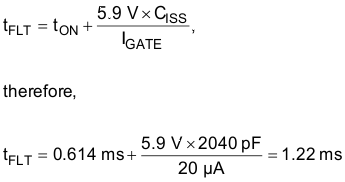
where CISS is the MOSFET input capacitance and IGATE is the minimum gate sourcing current of TPS24710/11/12/13, or 20 μA. Using the example parameters in Equation 12 and the CSD16403Q5 data sheet (SLPS201) leads to a minimum fault time of 1.22 ms. This time is derived considering the tolerances of COUT, CISS, ILIM, PLIM, IGATE, and VVCC(MAX). The fault timer must be set to a value higher than 1.22 ms to avoid turning off during start-up, but lower than any maximum fault time limit determined by the SOA curve (see Figure 38) derated for operating junction temperature.
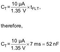
For this example, select 7 ms to allow for variation of system parameters such as temperature, load, component tolerance, and input voltage. The timing capacitor is calculated in Equation 5 as 52 nF. Selecting the next-highest standard value, 56 nF, yields a 7.56-ms fault time (see Equation 13).
9.2.2.1.5 STEP 5. Calculate the Retry-Mode Duty Ratio
In retry mode, the TPS24711/13 is on for one charging cycle and off for 16 charge/discharge cycles, as can be seen in Figure 33. The first CT charging cycle is from 0 V to 1.35 V, which gives 7.56 ms. The first CT discharging cycle is from 1.35 V to 0.35 V, which gives 5.6 ms. Therefore, the total time is 7.56 ms + 33 × 5.6 ms = 192.36 ms. As a result, the retry mode duty ratio is 7.56 ms/192.36 ms = 3.93%.
9.2.2.1.6 STEP 6. Select R1 and R2 for UV
Next, select the values of the UV resistors, R1 and R2, as shown in the typical application diagram on the front page. From the TPS24710/11/12/13 electrical specifications, VENTHRESH = 1.35 V. The VUV is the undervoltage trip voltage, which for this example equals 10.7 V.

Assume R1 is 130 kΩ and use Equation 14 to solve for the R2 value of 18.7 kΩ.
9.2.2.1.7 STEP 7. Choose RGATE, R4, R5 and C1
In the typical application diagram on the front page, the gate resistor, RGATE, is intended to suppress high-frequency oscillations. A resistor of 10 Ω will serve for most applications, but if M1 has a CISS below 200 pF, then 33 Ω is recommended. Applications with larger MOSFETs and very short wiring may not require RGATE. R4 and R5 are required only if PGb and FLTb are used; these resistors serve as pullups for the open-drain output drivers. The current sunk by each of these pins should not exceed 2 mA (see the RECOMMENDED OPERATING CONDITIONS table). C1 is a bypass capacitor to help control transient voltages, unit emissions, and local supply noise while in the disabled state. Where acceptable, a value in the range of 0.001 μF to 0.1 μF is recommended.
9.2.2.2 Additional Design Considerations
9.2.2.2.1 Use of PG/PGb
Use the PG/PGb pin to control and coordinate a downstream dc/dc converter. If this is not done, then a long time delay is needed to allow COUT to fully charge before the converter starts. An undesirable latch-up condition can be created between the TPS24710/11/12/13 output characteristic and the dc/dc converter input characteristic if the converter starts while COUT is still charging; the PG/PGb pin is one way to avoid this
9.2.2.2.2 Output Clamp Diode
Inductive loads on the output may drive the OUT pin below GND when the circuit is unplugged or during a current-limit event. The OUT pin ratings can be satisfied by connecting a diode from OUT to GND. The diode should be selected to control the negative voltage at the full short-circuit current. Schottky diodes are generally recommended for this application.
9.2.2.2.3 Gate Clamp Diode
The TPS24710/11/12/13 has a relatively well-regulated gate voltage of 12 V to 15.5 V with a supply voltage VVCC higher than 4 V. A small clamp Zener from GATE to source of M1 is recommended if VGS of M1 is rated below 12 V. A series resistance of several hundred ohms or a series silicon diode is recommended to prevent the output capacitance from discharging through the gate driver to ground.
9.2.2.2.4 High-Gate-Capacitance Applications
Gate voltage overstress and abnormally large fault current spikes can be caused by large gate capacitance. An external gate clamp Zener diode is recommended to assist the internal Zener if the total gate capacitance of M1 exceeds about 4000 pF.
9.2.2.2.5 Bypass Capacitors
It is a good practice to provide low-impedance ceramic capacitor bypassing of the VCC and OUT pins. Values in the range of 10 nF to 1 µF are recommended. Some system topologies are insensitive to the values of these capacitors; however, some are not and require minimization of the value of the bypass capacitor. Input capacitance on a plug-in board may cause a large inrush current as the capacitor charges through the low-impedance power bus when inserted. This stresses the connector contacts and causes a short voltage sag on the input bus. Small amounts of capacitance (e.g., 10 nF to 0.1 µF) are often tolerable in these systems.
9.2.2.2.6 Output Short-Circuit Measurements
Repeatable short-circuit testing results are difficult to obtain. The many details of source bypassing, input leads, circuit layout and component selection, output shorting method, relative location of the short, and instrumentation all contribute to variation in results. The actual short itself exhibits a certain degree of randomness as it microscopically bounces and arcs. Care in configuration and methods must be used to obtain realistic results. Do not expect to see waveforms exactly like those in this data sheet; every setup differs.
9.2.2.2.7 Using Soft Start with TPS2471x
In some applications, it may be desired to have a constant dv/dt ramp on the output of the TPS2471x to ensure a constant inrush current. This is often accomplished by adding a capacitor from GATE to GND as shown in Figure 37. This limits the gate ramp speed, which in turn limits the ramp of the output.
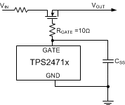 Figure 37. Simplified Diagram for Using Soft Start
Due to the nature of the timer and the gate driver, there are several considerations that must be taken into account when using this type of a design. For a further discussion of this topic, refer to the following Application Note: (SLVA749).
9.2.3 Application Curve
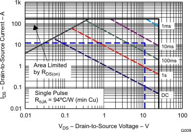 Figure 38. CSD16403Q5 SOA Curve