-
TPS2471x 2.5-V to 18-V High-Efficiency Power-Limiting Hot-Swap Controller
- 1 Features
- 2 Applications
- 3 Description
- 4 Revision History
- 5 Device Comparison Table
- 6 Pin Configuration and Functions
- 7 Specifications
- 8 Detailed Description
-
9 Application and Implementation
- 9.1 Application Information
- 9.2
Typical Application
- 9.2.1 Design Requirements
- 9.2.2
Detailed Design Procedure
- 9.2.2.1
Power-Limited Start-Up
- 9.2.2.1.1 STEP 1. Choose RSENSE
- 9.2.2.1.2 STEP 2. Choose MOSFET M1
- 9.2.2.1.3 STEP 3. Choose Power-Limit Value, PLIM, and RPROG
- 9.2.2.1.4 STEP 4. Choose Output Voltage Rising Time, tON, CT
- 9.2.2.1.5 STEP 5. Calculate the Retry-Mode Duty Ratio
- 9.2.2.1.6 STEP 6. Select R1 and R2 for UV
- 9.2.2.1.7 STEP 7. Choose RGATE, R4, R5 and C1
- 9.2.2.2 Additional Design Considerations
- 9.2.2.1
Power-Limited Start-Up
- 9.2.3 Application Curve
- 10Power Supply Recommendations
- 11Layout
- 12Device and Documentation Support
- 13Mechanical, Packaging, and Orderable Information
- IMPORTANT NOTICE
TPS2471x 2.5-V to 18-V High-Efficiency Power-Limiting Hot-Swap Controller
1 Features
- 2.5-V to 18-V Operation
- Accurate Current Limiting for Startup
- Programmable FET SOA Protection
- Accurate 25-mV Current-Sense Threshold
- Power-Good Output
- Fast Breaker for Short-Circuit Protection
- Programmable Fault Timer
- Programmable UV Threshold
- Drop-In Upgrade for LTC4211 – No Layout Changes
- PG, FLT Active-High and Active-Low Versions
- MSOP-10 Package
2 Applications
- Server Backplanes
- Storage Area Networks (SAN)
- Medical Systems
- Plug-In Modules
- Base Stations
3 Description
The TPS24710/11/12/13 is an easy-to-use, 2.5 V to 18 V, hot-swap controller that safely drives an external N-channel MOSFET. The programmable current limit and fault time protect the supply and load from excessive current at startup. After startup, currents above the user-selected limit will be allowed to flow until programmed timeout – except in extreme overload events when the load is immediately disconnected from source. The low, 25mV current sense threshold is highly accurate and allows use of smaller, more efficient sense resistors yielding lower power loss and smaller footprint.
Programmable power limiting ensures the external MOSFET operates inside its safe operating area (SOA) at all times. This allows the use of smaller MOSFETS while improving system reliability. Power good and fault outputs are provided for status monitoring and downstream load control.
Device Information(1)
| PART NUMBER | PACKAGE | BODY SIZE (NOM) |
|---|---|---|
| TPS24710 | SSOP (10) | 3.00 mm × 3.00 mm |
| TPS24711 | ||
| TPS24712 | ||
| TPS24713 |
- For all available packages, see the orderable addendum at the end of the data sheet.
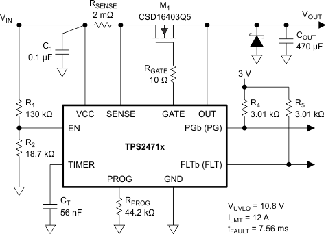
Typical Application (12 V at 10 A)
4 Revision History
Changes from F Revision (February 2015) to G Revision
- Changed the values of the Power limit threshold in Electrical Characteristics for VOUT = 7 V and VOUT = 2 V From: 10, 12.5, 15 mV To: 10.1, 11.6, 13.1 mVGo
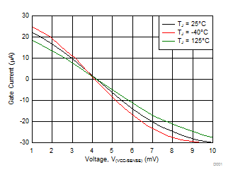
- Changed the title of Figure 8 From: MOSFET Gate Current vs Voltage Across RSENSE During Inrush Power Limiting To: Gate Current vs Voltage Across RSENSEGo
- Added Figure 9 Go
- Changed V(VCC–SENSE) To: V(SENSE–VCC) in Figure 10 and Figure 11Go
- Added Equation 1 Go
- Added text to the PROG section: "To compute the Power limit based on an existing RPROG..." Go
- Changed Equation 2 Go
- Changed text in STEP 3. Choose Power-Limit Value, PLIM, and RPROG From: "a 53.6-kΩ, 1% resistor is selected for RPROG" To: a 44.2-kΩ, 1% resistor is selected for RPROG"Go
- Changed Equation 9 Go
- Added the Using Soft Start with TPS2471x section Go
Changes from E Revision (November 2013) to F Revision
- Added ESD Rating table, Feature Description section, Device Functional Modes, Application and Implementation section, Power Supply Recommendations section, Layout section, Device and Documentation Support section, and Mechanical, Packaging, and Orderable Information section. Go
- Changed the Input voltage range, PROG - MAX value in the Absolute Maximum Ratings table From: 0.3 To: 3.6 Go
- Deleted External capacitance - GATE from the Recommended Operating ConditionsGo
- Deleted text from the last paragraph in the GATE section "If used, any capacitor connecting GATE and GND should not exceed 1 μF and it should be connected in series with a resistor of no less than 1 kΩ."Go
- Deleted section: Alternative Design Example: GATE Capacitor (dV/dt) Control in Inrush ModeGo
- Deleted text from the High-Gate-Capacitance Applications section "When gate capacitor dV/dt control is used, ... then a Zener diode is not necessary."Go
Changes from D Revision (November 2013) to E Revision
- Reverted Equation 2 in rev E back to rev CGo
- Reverted Equation 9 in rev E back to rev CGo
Changes from C Revision (May 2011) to D Revision
- Added Note 1 to the Supply Current Conditions statementGo
- Added Note 1 to Fast-turnoff delay Go
- Changed the Functional Block Diagram From: VCC = 6 V to VCC = 5.9 V at the Gate ComparatorGo
- Changed text in the GATE section From: "Timer Activation Voltage (6 V for VVCC = 12 V)." To: "Timer Activation Voltage (5.9 V for VVCC = 12 V)."Go
- Changed the first paragraph of the Inrush Operation sectionGo
- Added text and new Equation 10Go
- Changed text prior to Equation 12 From: "6 V (for VVCC = 12 V)" To: "5.9 V (for VVCC = 12 V)"Go
- Changed the text following Equation 12Go
- Changed text following Alternative Design Example: GATE Capacitor (dV/dt) Control in Inrush Mode From: "Set PLIM to a value greater than VVCC × ICHG" To: "Choose ICHG < PLIM / VVCC"Go
- Changed Equation 15 From: – CISS To: – CRS (this equation deleted by Revision F)Go
Changes from B Revision (April 2011) to C Revision
Changes from A Revision (March 2011) to B Revision
5 Device Comparison Table
| TPS24710 | TPS24711 | TPS24712 | TPS24713 | |
|---|---|---|---|---|
| Latch Off | X | X | ||
| Retry | X | X | ||
| PG | L | L | H | H |
| FLT | L | L | H | H |
6 Pin Configuration and Functions
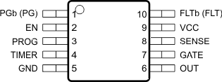
Pin Functions
| PINS | I/O | DESCRIPTION | ||
|---|---|---|---|---|
| NAME | TPS24710/11 | TPS24712/13 | ||
| EN | 2 | 2 | I | Active-high enable input. Logic input. Connects to resistor divider. |
| FLT | – | 10 | O | Active-high, open-drain output indicates overload fault timer has turned MOSFET off. |
| FLTb | 10 | – | Active-low, open-drain output indicates overload fault timer has turned MOSFET off. | |
| GATE | 7 | 7 | O | Gate driver output for external MOSFET |
| GND | 5 | 5 | – | Ground |
| OUT | 6 | 6 | I | Output voltage sensor for monitoring MOSFET power. |
| PG | – | 1 | O | Active-high, open-drain power good indicator. Status is determined by the voltage across the MOSFET. |
| PGb | 1 | – | Active-low, open-drain power good indicator. Status is determined by the voltage across the MOSFET. | |
| PROG | 3 | 3 | I | Power-limiting programming pin. A resistor from this pin to GND sets the maximum power dissipation for the FET. |
| SENSE | 8 | 8 | I | Current sensing input for resistor shunt from VCC to SENSE. |
| TIMER | 4 | 4 | I/O | A capacitor connected from this pin to GND provides a fault timing function. |
| VCC | 9 | 9 | I | Input-voltage sense and power supply |
7 Specifications
7.1 Absolute Maximum Ratings
over operating free-air temperature range, all voltages referred to GND (unless otherwise noted) (1)| MIN | MAX | UNIT | |||
|---|---|---|---|---|---|
| Input voltage range | EN, FLT(2)(3), FLTb(2)(4), GATE, OUT, PG(2)(3), PGb(2)(4), SENSE, VCC | –0.3 | 30 | V | |
| PROG(2) | –0.3 | 3.6 | |||
| SENSE to VCC | –0.3 | 0.3 | |||
| TIMER | –0.3 | 5 | |||
| Sink current | FLT, PG, FLTb, PGb | 5 | mA | ||
| Source current | PROG | Internally limited | |||
| Temperature | Maximum junction, TJ | Internally limited | °C | ||
7.2 ESD Ratings
| VALUE | UNIT | ||||
|---|---|---|---|---|---|
| V(ESD) | Electrostatic discharge | Human-body model (HBM), per ANSI/ESDA/JEDEC JS-001(1) | All pins except PG and PGb | ±2000 | V |
| PG, PGb | ±500 | V | |||
| Charged-device model (CDM), per JEDEC specification JESD22-C101(2) | ±500 | V | |||
7.3 Recommended Operating Conditions
over operating free-air temperature range (unless otherwise noted)| MIN | NOM | MAX | UNIT | ||
|---|---|---|---|---|---|
| Input voltage range | SENSE, VCC | 2.5 | 18 | V | |
| EN, FLT, FLTb, PG, PGb, OUT | 0 | 18 | |||
| Sink current | FLT, FLTb, PG, PGb | 0 | 2 | mA | |
| Resistance | PROG | 4.99 | 500 | kΩ | |
| External capacitance | TIMER | 1 | nF | ||
| Operating junction temperature range, TJ | –40 | 125 | °C | ||
7.4 Thermal Information
| THERMAL METRIC(1) | TPS2471/x | UNIT | |
|---|---|---|---|
| MSOP (10) PINS | |||
| RθJA | Junction-to-ambient thermal resistance | 166.5 | °C/W |
| RθJC(top) | Junction-to-case (top) thermal resistance | 41.8 | |
| RθJB | Junction-to-board thermal resistance | 86.1 | |
| ψJT | Junction-to-top characterization parameter | 1.5 | |
| ψJB | Junction-to-board characterization parameter | 84.7 | |
| RθJC(bot) | Junction-to-case (bottom) thermal resistance | n/a | |
7.5 Electrical Characteristics
–40°C ≤ TJ ≤ 125°C, VCC = 12 V, VEN = 3 V, and RPROG = 50 kΩ to GND.All voltages referenced to GND, unless otherwise noted.
| PARAMETER | CONDITIONS | MIN | NOM | MAX | UNIT |
|---|---|---|---|---|---|
| VCC | |||||
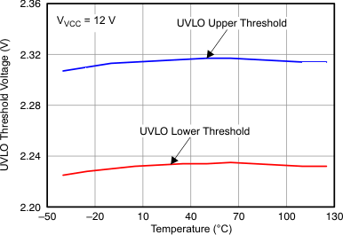
| UVLO threshold, rising | 2.2 | 2.32 | 2.45 | V | |
| UVLO threshold, falling | 2.1 | 2.22 | 2.35 | V | |
| UVLO hysteresis(1) | 0.1 | V | |||
| Supply current | Enabled ― IOUT + IVCC + ISENSE | 1 | 1.4 | mA | |
| Disabled(1) ― EN = 0 V, IOUT + IVCC + ISENSE | 0.45 | mA | |||
| EN | |||||
| Threshold voltage, falling | 1.2 | 1.3 | 1.4 | V | |
| Hysteresis(1) | 50 | mV | |||
| Input leakage current | 0 V ≤ VEN ≤ 30 V | –1 | 0 | 1 | µA |
| FLT, FLTb | |||||
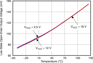
| Output low voltage | Sinking 2 mA | 0.11 | 0.25 | V | |
| Input leakage current | VFLT = 0 V, 30 V | –1 | 0 | 1 | µA |
| VFLTb = 0 V, 30 V | |||||
| PG, PGb | |||||
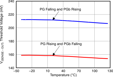
| Threshold | V(SENSE – OUT) rising, PG going low | 140 | 240 | 340 | mV |
| V(SENSE – OUT) rising, PGb going high | |||||
| Hysteresis(1) | Measured V(SENSE – OUT) falling, PG going high | 70 | mV | ||
| Measured V(SENSE – OUT) falling, PGb going low | |||||
| Output low voltage | Sinking 2 mA | 0.11 | 0.25 | V | |
| Input leakage current | VPG = 0 V, 30 V | –1 | 0 | 1 | µA |
| VPGb = 0 V, 30 V | |||||
| PROG | |||||
| Bias voltage | Sourcing 10 µA | 0.65 | 0.678 | 0.7 | V |
| Input leakage current | VPROG = 1.5 V | –0.2 | 0 | 0.2 | µA |
| TIMER | |||||
| Sourcing current | VTIMER = 0 V | 8 | 10 | 12 | µA |
| Sinking current | VTIMER = 2 V | 8 | 10 | 12 | µA |
| VEN = 0 V, VTIMER = 2 V | 2 | 4.5 | 7 | mA | |
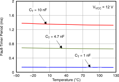
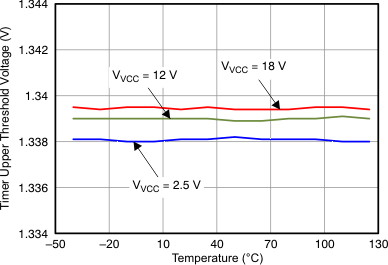
| Upper threshold voltage | 1.30 | 1.35 | 1.40 | V | |
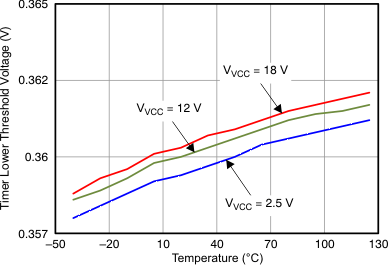
| Lower threshold voltage | 0.33 | 0.35 | 0.37 | V | |
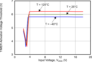
| Timer activation voltage | Raise GATE until ITIMER sinking, measure V(GATE – VCC), VCC = 12 V | 5 | 5.9 | 7 | V |
| Bleed-down resistance | VENSD = 0 V, VTIMER = 2 V | 70 | 104 | 130 | kΩ |
| OUT | |||||
| Input bias current | VOUT = 12 V | 16 | 30 | µA | |
| GATE | |||||
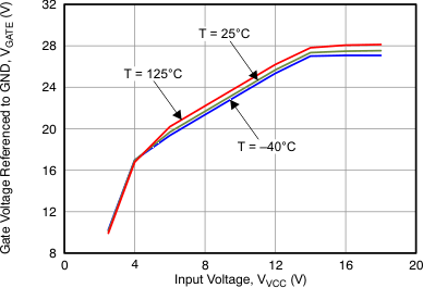
| Output voltage | VOUT = 12 V | 23.5 | 25.8 | 28 | V |
| Clamp voltage | Inject 10 µA into GATE, measure V(GATE – VCC) | 12 | 13.9 | 15.5 | V |
| Sourcing current | VGATE = 12 V | 20 | 30 | 40 | µA |
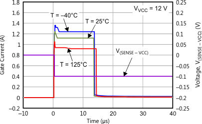
| Sinking current | Fast turnoff, VGATE = 14 V | 0.5 | 1 | 1.4 | A |
| Sustained, VGATE = 4 V to 23 V | 6 | 11 | 20 | mA | |
| In inrush current limit, VGATE = 4 V to 23 V | 20 | 30 | 40 | µA | |
| Pulldown resistance | Thermal shutdown | 14 | 20 | 26 | kΩ |
| SENSE | |||||
| Input bias current | VSENSE = 12 V, sinking current | 30 | 40 | µA | |
| Current limit threshold | VOUT = 12 V | 22.5 | 25 | 27.5 | mV |
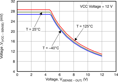
| Power limit threshold | VOUT = 7 V, RPROG = 50 kΩ | 10.1 | 11.6 | 13.1 | mV |
| VOUT = 2 V, RPROG = 25 kΩ | 10.1 | 11.6 | 13.1 | ||
| Fast-trip threshold | 52 | 60 | 68 | mV | |
| OTSD | |||||
| Threshold, rising | 130 | 140 | °C | ||
| Hysteresis(1) | 10 | °C | |||
7.6 Timing Requirements
| MIN | NOM | MAX | UNIT | ||
|---|---|---|---|---|---|
| EN | |||||
| Turnoff time | EN ↓ to VGATE < 1 V, CGATE = 33 nF | 20 | 60 | 150 | µs |
| Deglitch time | EN ↑ | 8 | 14 | 18 | µs |
| Disable delay | EN ↓ to GATE ↓, CGATE = 0, tpff50–90, See Figure 1 | 0.1 | 0.4 | 1 | µs |
| PG, PGb | |||||
| Delay (deglitch) time | Rising or falling edge | 2 | 3.4 | 6 | ms |
| GATE | |||||
| Fast-turnoff duration | 8 | 13.5 | 18 | µs | |
| Turn on delay | VCC rising to GATE sourcing, tprr50-50, See Figure 2 | 100 | 250 | µs | |
| SENSE | |||||
| Fast-turnoff duration | 8 | 13.5 | 18 | µs | |
| Fast-turnoff delay(1) | V(VCC – SENSE) = 80 mV, CGATE = 0 pF, tprf50–50, See Figure 3 | 200 | ns | ||
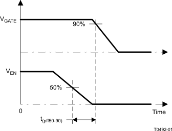 Figure 1. tpff50–90 Timing Definition
 Figure 2. tprr50–50 Timing Definition
 Figure 3. tprf50–50 Timing Definition
7.7 Typical Characteristics

| EN = High |





| EN = 0 V |

| VVCC = VGATE = 3.3 V | ||
