SLVSAL2G January 2011 – November 2015 TPS24710 , TPS24711 , TPS24712 , TPS24713
PRODUCTION DATA.
- 1 Features
- 2 Applications
- 3 Description
- 4 Revision History
- 5 Device Comparison Table
- 6 Pin Configuration and Functions
- 7 Specifications
- 8 Detailed Description
-
9 Application and Implementation
- 9.1 Application Information
- 9.2
Typical Application
- 9.2.1 Design Requirements
- 9.2.2
Detailed Design Procedure
- 9.2.2.1
Power-Limited Start-Up
- 9.2.2.1.1 STEP 1. Choose RSENSE
- 9.2.2.1.2 STEP 2. Choose MOSFET M1
- 9.2.2.1.3 STEP 3. Choose Power-Limit Value, PLIM, and RPROG
- 9.2.2.1.4 STEP 4. Choose Output Voltage Rising Time, tON, CT
- 9.2.2.1.5 STEP 5. Calculate the Retry-Mode Duty Ratio
- 9.2.2.1.6 STEP 6. Select R1 and R2 for UV
- 9.2.2.1.7 STEP 7. Choose RGATE, R4, R5 and C1
- 9.2.2.2 Additional Design Considerations
- 9.2.2.1
Power-Limited Start-Up
- 9.2.3 Application Curve
- 10Power Supply Recommendations
- 11Layout
- 12Device and Documentation Support
- 13Mechanical, Packaging, and Orderable Information
1 Features
- 2.5-V to 18-V Operation
- Accurate Current Limiting for Startup
- Programmable FET SOA Protection
- Accurate 25-mV Current-Sense Threshold
- Power-Good Output
- Fast Breaker for Short-Circuit Protection
- Programmable Fault Timer
- Programmable UV Threshold
- Drop-In Upgrade for LTC4211 – No Layout Changes
- PG, FLT Active-High and Active-Low Versions
- MSOP-10 Package
2 Applications
- Server Backplanes
- Storage Area Networks (SAN)
- Medical Systems
- Plug-In Modules
- Base Stations
3 Description
The TPS24710/11/12/13 is an easy-to-use, 2.5 V to 18 V, hot-swap controller that safely drives an external N-channel MOSFET. The programmable current limit and fault time protect the supply and load from excessive current at startup. After startup, currents above the user-selected limit will be allowed to flow until programmed timeout – except in extreme overload events when the load is immediately disconnected from source. The low, 25mV current sense threshold is highly accurate and allows use of smaller, more efficient sense resistors yielding lower power loss and smaller footprint.
Programmable power limiting ensures the external MOSFET operates inside its safe operating area (SOA) at all times. This allows the use of smaller MOSFETS while improving system reliability. Power good and fault outputs are provided for status monitoring and downstream load control.
Device Information(1)
| PART NUMBER | PACKAGE | BODY SIZE (NOM) |
|---|---|---|
| TPS24710 | SSOP (10) | 3.00 mm × 3.00 mm |
| TPS24711 | ||
| TPS24712 | ||
| TPS24713 |
- For all available packages, see the orderable addendum at the end of the data sheet.
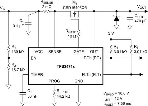
Typical Application (12 V at 10 A)
