SLVSCV6A January 2015 – February 2015 TPS24740 , TPS24741 , TPS24742
PRODUCTION DATA.
- 1 Features
- 2 Applications
- 3 Description
- 4 Simplified Schematics
- 5 Revision History
- 6 Device Comparison Table
- 7 Pin Configuration and Functions
- 8 Specifications
-
9 Detailed Description
- 9.1 Overview
- 9.2 Functional Block Diagram
- 9.3
Feature Description
- 9.3.1 Internal Power ORing of TPS24740
- 9.3.2 Enable and Over-voltage Protection
- 9.3.3 Current Limit and Power Limit During Start-up
- 9.3.4 Two Level Protection During Regular Operation
- 9.3.5 Dual Timer (TFLT and TINR)
- 9.3.6 Using SoftStart - IHGATE and TINR Considerations
- 9.3.7 Three Options for Response to a Fast Trip
- 9.3.8 Programmable Reverse Voltage Threshold
- 9.3.9 Analog Current Monitor
- 9.3.10 Power Good Flag
- 9.3.11 ORing MOSFET Status Indicator
- 9.3.12 Fault Reporting
- 9.4 Device Functional Modes
-
10Application and Implementation
- 10.1 Application Information
- 10.2
Typical Application
- 10.2.1 30A Single channel OR then Hot Swap With Current Monitoring
- 10.2.2 Design Requirements
- 10.2.3
Detailed Design Procedure
- 10.2.3.1 Select RSNS and VSNS,CL Setting
- 10.2.3.2 Selecting the Fast Trip Threshold and Filtering
- 10.2.3.3 Selecting the Hot Swap FET(s)
- 10.2.3.4 Select Power Limit
- 10.2.3.5 Set Fault Timer
- 10.2.3.6 Check MOSFET SOA
- 10.2.3.7 Choose ORing MOSFET
- 10.2.3.8 Choose Reverse Current Threshold and Filtering
- 10.2.3.9 Choose Under Voltage and Over Voltage Settings
- 10.2.3.10 Selecting CIN, COUT, and CMIDDLE
- 10.2.3.11 Selecting D1 and D2
- 10.2.3.12 Ensuring Stability
- 10.2.3.13 Compute Tolerances
- 10.2.4 Application Curves
- 10.2.5
40 A Single Channel Hot Swap then ORing
- 10.2.5.1 Design Requirements
- 10.2.5.2
Design Procedure
- 10.2.5.2.1 Select RSNS and VSNS,CL Setting
- 10.2.5.2.2 Selecting the Fast Trip Threshold and Filtering
- 10.2.5.2.3 Selecting the Hot Swap FET
- 10.2.5.2.4 Select Power Limit
- 10.2.5.2.5 Set Fault Timer
- 10.2.5.2.6 Check MOSFET SOA
- 10.2.5.2.7 Checking Stability of Hot Swap Loop
- 10.2.5.2.8 Choose ORing MOSFET
- 10.2.5.2.9 Choose Reverse Current Threshold and Filtering
- 10.2.5.2.10 Choose Under Voltage and Over Voltage Settings
- 10.2.5.2.11 Selecting CIN, COUT, CMIDDLE, and Transient Protection
- 10.2.5.2.12 Adding CENHS
- 10.2.5.3 Application Curves
- 10.3 System Examples
- 11Power Supply Recommendations
- 12Layout
- 13Device and Documentation Support
- 14Mechanical, Packaging, and Orderable Information
パッケージ・オプション
メカニカル・データ(パッケージ|ピン)
- RGE|24
サーマルパッド・メカニカル・データ
- RGE|24
発注情報
12 Layout
12.1 Layout Guidelines
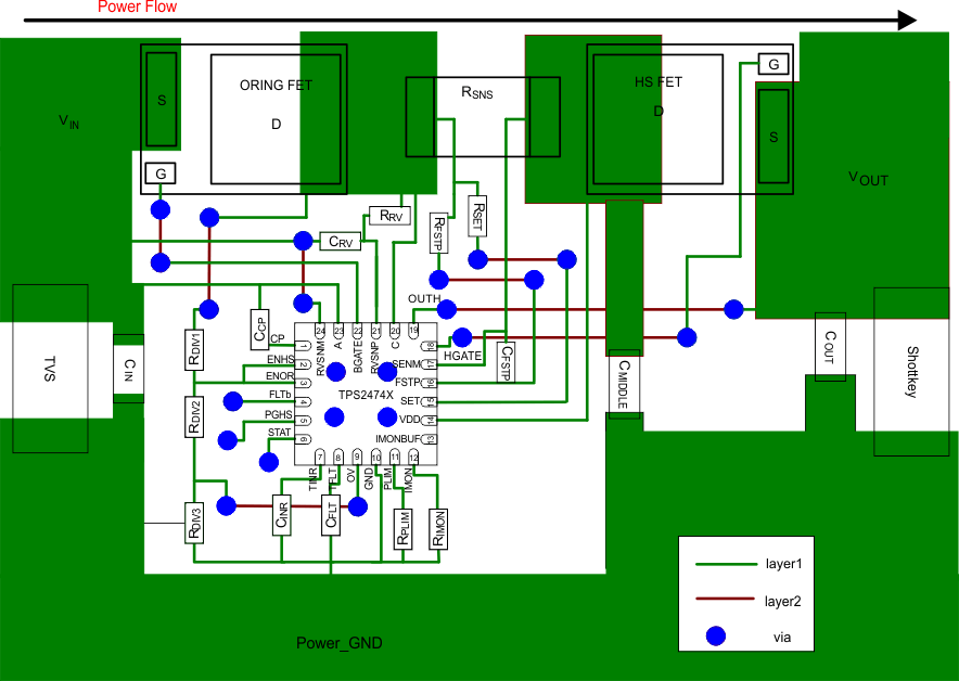
When doing the layout of the TPS2474x in the ORing then hot swap configuration the following are considered best practice.
- Ensure proper Kelvin Sense of RSNS
- Keep the filtering capacitors CFSTP and CRV as close to the IC as possible.
- Keep the traces from CCP to CP and A as short as possible.
- Run a separate trace from A and RVSNM to ORing FET source. This will prevent the charge pump noise along with a DC bias (due to supply current draw) from interfering with the reverse current threshold.
- Run a separate trace from C and from RRV to ORing FET drain.
- Place a Schottky diode and a ceramic bypass capacitor close to the source of the Hot Swap MOSFET.
- Place a TVS and a ceramic bypass capacitor between VIN and ground close to the source of the ORing MOSFET.
- Use a separate trace to connect to VDD and SENM.
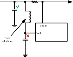
- Note that special care must be taken when placing the bypass capacitor for the VDD pin. During Hot Shorts, there is a very large dv/dt on input voltage during the MOSFET turn off. If the bypass capacitor is placed right next to the pin and the trace from RSNS to the pin is long, an LC filter is formed. As a result a large differential voltage can develop between VDD and SENM if there is a large transient on Vin. This could result in a violation of the abs max rating from VDD to SENM. To avoid this, place the bypass capacitor close to RSNS instead of the VDD pin.
 Figure 75. Layout Don'ts
12.2 Layout Example
 Figure 76. Layout Example for ORing then Hot Swap Configuration