JAJSGL9C October 2013 – December 2018 TPS24750 , TPS24751
UNLESS OTHERWISE NOTED, this document contains PRODUCTION DATA.
- 1 特長
- 2 アプリケーション
- 3 概要
- 4 改訂履歴
- 5 Device Comparison Table
- 6 Pin Configuration and Functions
- 7 Specifications
- 8 Parameter Measurement Information
-
9 Detailed Descriptions
- 9.1 Overview
- 9.2 Functional Block Diagram
- 9.3 Feature Description
- 9.4 Device Functional Modes
-
10Application and Implementation
- 10.1 Application Information
- 10.2
Typical Application
- 10.2.1 Design Requirements
- 10.2.2
Detailed Design Procedure
- 10.2.2.1
Power-Limited Start-Up
- 10.2.2.1.1 STEP 1. Choose RSENSE, RSET, and RIMON
- 10.2.2.1.2 STEP 2. Choose Power-Limit Value, PLIM, and RPROG
- 10.2.2.1.3 STEP 3. Choose Output Voltage Rising Time, tON, and Timing Capacitor CT
- 10.2.2.1.4 STEP 4. Calculate the Retry-Mode Duty Ratio
- 10.2.2.1.5 STEP 5. Select R1, R2, and R3 for UV and OV
- 10.2.2.1.6 STEP 6. Choose R4, R5, and C1
- 10.2.2.2 Alternative Design Example: Gate Capacitor (dv/dt) Control in Inrush Mode
- 10.2.2.3 Additional Design Considerations
- 10.2.2.1
Power-Limited Start-Up
- 10.2.3 Application Curves
- 10.3 System Examples
- 11Power Supply Recommendations
- 12Layout
- 13デバイスおよびドキュメントのサポート
- 14メカニカル、パッケージ、および注文情報
パッケージ・オプション
メカニカル・データ(パッケージ|ピン)
- RUV|36
サーマルパッド・メカニカル・データ
- RUV|36
発注情報
9.4.4 Circuit Breaker and Fast Trip
The TPS2475x monitors load current by sensing the voltage across RSENSE. The TPS2475x incorporates two distinct thresholds: a current-limit threshold and a fast-trip threshold.
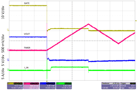
The functions of circuit breaker and fast-trip turnoff are shown in Figure 33 through Figure 36.
Figure 33 shows the behavior of the TPS2475x when a fault in the output load causes the current passing through RSENSE to increase to a value above the current limit but less than the fast-trip threshold. When the current exceeds the current-limit threshold, a current of approximately 10 μA begins to charge timing capacitor CT. If the voltage on CT reaches 1.35 V, then the internal FET is turned off. The TPS24750 version latches off, while as the TPS24751 version commences a restart cycle. In either event, fault pin FLTb pulls low to signal a fault condition. Overload between the current limit and the fast-trip threshold is permitted for this period. This shutdown scheme is sometimes called an electronic circuit breaker.
The fast-trip threshold protects the system against a severe overload or a dead short circuit. When the voltage across the sense resistor RSENSE exceeds the 60-mV fast-trip threshold, the GATE pin immediately pulls the internal FET gate to ground with approximately 1 A of current. The fast-trip circuit holds the internal FET off for only a few microseconds, after which the TPS2475x turns back on slowly, allowing the current-limit feedback loop to take over the gate control of the internal FET. Then the hot-swap circuit goes into latch mode (TPS24750) or auto-retry mode (TPS24751). Figure 35 and Figure 36 illustrate the behavior of the system when the current exceeds the fast-trip threshold.
 Figure 33. Circuit-Breaker Mode During Overload Condition
  Figure 34. Partial Diagram of the TPS2475x with Selected External Components
  Figure 35. Current Limit During Output-Load Short-Circuit Condition (Overview)
  Figure 36. Current Limit During Output-Load Short-Circuit Condition (Onset)