JAJSGL9C October 2013 – December 2018 TPS24750 , TPS24751
UNLESS OTHERWISE NOTED, this document contains PRODUCTION DATA.
- 1 特長
- 2 アプリケーション
- 3 概要
- 4 改訂履歴
- 5 Device Comparison Table
- 6 Pin Configuration and Functions
- 7 Specifications
- 8 Parameter Measurement Information
-
9 Detailed Descriptions
- 9.1 Overview
- 9.2 Functional Block Diagram
- 9.3 Feature Description
- 9.4 Device Functional Modes
-
10Application and Implementation
- 10.1 Application Information
- 10.2
Typical Application
- 10.2.1 Design Requirements
- 10.2.2
Detailed Design Procedure
- 10.2.2.1
Power-Limited Start-Up
- 10.2.2.1.1 STEP 1. Choose RSENSE, RSET, and RIMON
- 10.2.2.1.2 STEP 2. Choose Power-Limit Value, PLIM, and RPROG
- 10.2.2.1.3 STEP 3. Choose Output Voltage Rising Time, tON, and Timing Capacitor CT
- 10.2.2.1.4 STEP 4. Calculate the Retry-Mode Duty Ratio
- 10.2.2.1.5 STEP 5. Select R1, R2, and R3 for UV and OV
- 10.2.2.1.6 STEP 6. Choose R4, R5, and C1
- 10.2.2.2 Alternative Design Example: Gate Capacitor (dv/dt) Control in Inrush Mode
- 10.2.2.3 Additional Design Considerations
- 10.2.2.1
Power-Limited Start-Up
- 10.2.3 Application Curves
- 10.3 System Examples
- 11Power Supply Recommendations
- 12Layout
- 13デバイスおよびドキュメントのサポート
- 14メカニカル、パッケージ、および注文情報
パッケージ・オプション
メカニカル・データ(パッケージ|ピン)
- RUV|36
サーマルパッド・メカニカル・データ
- RUV|36
発注情報
9.4.6 Start-Up with Short on Output
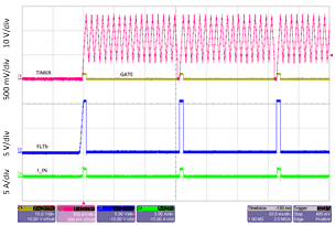
The TPS2475x has ability of detecting the short at the output during start-up and ensure shutdown of the hot-swap circuit/system with fault indication. During start-up, after the initialization process is complete and the GATE is enabled, the device limits the power as explained in the Action of the Constant-Power Engine section and the TIMER pin begins to charge the timing capacitor CT with approximately 10 µA constant current source. If the voltage on CT reaches its upper limit threshold of 1.35V, during start-up cycle itself, then the internal FET is turned off and fault pin FLTb is pulled low to signal the fault condition. After this, the hot-swap circuit enters either in latch mode (TPS24750) or auto-retry mode (TPS24751). Figure 39 shows the behavior of the TPS2475x for start-up with short on the output.
This feature help to ensure early detection of fault and quick isolation of the subsystem to ensure stability of the other units connected on the DC bus.
 Figure 39. Start-Up with Short on Output