SLVSCZ3 March 2015 TPS24770 , TPS24771 , TPS24772
PRODUCTION DATA.
- 1 Features
- 2 Applications
- 3 Description
- 4 Simplified Schematic
- 5 Revision History
- 6 Device Comparison Table
- 7 Pin Configuration and Functions
- 8 Specifications
-
9 Detailed Description
- 9.1 Overview
- 9.2 Functional Block Diagram
- 9.3
Feature Description
- 9.3.1 Enable and Over-voltage Protection
- 9.3.2 Current Limit and Power Limit during Start-up
- 9.3.3 Two Level Protection During Regular Operation
- 9.3.4 Dual Timer (TFLT and TINR)
- 9.3.5 3 Options for Response to a Fast Trip
- 9.3.6 Using Soft Start - IHGATE and TINR Considerations
- 9.3.7 Analog Current Monitor
- 9.3.8 Power Good Flag
- 9.3.9 Fault Reporting
- 9.4 Device Functional Modes
-
10Application and Implementation
- 10.1 Application Information
- 10.2
Typical Application
- 10.2.1 12 V, 100 A, 5,500 µF Analog Hot Swap Design
- 10.2.2 Design Requirements
- 10.2.3
Detailed Design Procedure
- 10.2.3.1 Select RSNS and VSNS,CL Setting
- 10.2.3.2 Selecting the Fast Trip Threshold and Filtering
- 10.2.3.3 Selecting the Hot Swap FET(s)
- 10.2.3.4 Select Power Limit
- 10.2.3.5 Set Fault Timer
- 10.2.3.6 Check MOSFET SOA
- 10.2.3.7 Choose Under Voltage and Over Voltage Settings
- 10.2.3.8 Selecting C1 and COUT
- 10.2.3.9 Adding CENHS
- 10.2.3.10 Selecting D1 and D2
- 10.2.3.11 Checking Stability
- 10.2.3.12 Compute Tolerances
- 10.2.4 Application Curves
- 10.2.5
240 VA Application Using CSD16415Q5B
- 10.2.5.1 Design Requirements
- 10.2.5.2 Theory of Operations
- 10.2.5.3
Design Procedure
- 10.2.5.3.1
Select VSNS,CL, RSNS, and RSET Setting
- 10.2.5.3.1.1 Select RPOW and RIMON
- 10.2.5.3.1.2 Selecting the Hot Swap FET(s)
- 10.2.5.3.1.3 Keeping MOSFET within SOA During Normal Start-up
- 10.2.5.3.1.4 Choose Fault Timer
- 10.2.5.3.1.5 Choose Under Voltage and Over Voltage Settings
- 10.2.5.3.1.6 Selecting CIN and COUT
- 10.2.5.3.1.7 Selecting D1 and D2
- 10.2.5.3.1.8 Adding CENHS
- 10.2.5.3.1.9 Stability Considerations
- 10.2.5.3.1
Select VSNS,CL, RSNS, and RSET Setting
- 10.2.5.4 Application Curves
- 10.2.6 240 VA Application Using CSD17573Q5B
- 11Power Supply Recommendations
- 12Layout
- 13Device and Documentation Support
- 14Mechanical, Packaging, and Orderable Information
パッケージ・オプション
メカニカル・データ(パッケージ|ピン)
- RGE|24
サーマルパッド・メカニカル・データ
- RGE|24
発注情報
10 Application and Implementation
NOTE
Information in the following applications sections is not part of the TI component specification, and TI does not warrant its accuracy or completeness. TI’s customers are responsible for determining suitability of components for their purposes. Customers should validate and test their design implementation to confirm system functionality.
10.1 Application Information
The TPS2477x is a highly configurable Hot Swap controller that can be fine-tuned for the application requirement. When designing a Hot Swap 3 key scenarios should be considered:
- Start-up.
- Output of a Hot Swap is shorted to ground when the Hot Swap is on. This is often referred to as a “Hot-Short”.
- Powering up a board when the output and ground are shorted. This is usually called a “start into short”.
All of these scenarios place a lot of stress on the Hot Swap MOSFET and special care must be taken when designing the Hot Swap circuit to keep the MOSFET within its Safe Operating Area (SOA). Note that the component selection can often be iteratively and it’s recommended to use the publically available excel calculators to crunch the numbers. See the TPS24770 Design Calculator in the Tools & Software link on the Product folder.
10.2 Typical Application
Three application examples are provided. The first one is for a 100A Hot Swap with 5,500 µF of output capacitance that uses standard power limited based start-up. Then there are two examples of designing for the 240 VA design requirment. One uses the CSD16415Q5B, which is an older generation MOFSET with great SOA. The second one uses the CSD17573Q5B, which has lower SOA, but is more cost effective (price vs RDSON).
10.2.1 12 V, 100 A, 5,500 µF Analog Hot Swap Design
The diagram below shows the application schematic for this design example.
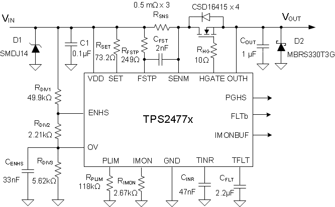 Figure 18. Application Schematic for 100 A Hot Swap
10.2.2 Design Requirements
Table 1 summarizes the design parameters that must be known before designing a Hot Swap circuit. When charging the output capacitor through the Hot Swap MOSFET, the FET’s total energy dissipation equals the total energy stored in the output capacitor (1/2CV2). Thus both the input voltage and output capacitance will determine the stress experienced by the MOSFET. The maximum load current will drive the current limit and sense resistor selection. In addition, the maximum load current, maximum ambient temperature, and the thermal properties of the PCB (RθCA) will drive the selection of the MOSFET RDSON and the number of MOSFETs used. RθCA is a strong function of the layout and the amount of copper that is connected to the drain of the MOSFET. Air cooling will also reduce RθCA. It’s also important to know if there are any transient load requirements. Finally, whether current monitoring is needed and its accuracy requirement will drive the selection of RSNS, RIMON, and RSET.
Table 1. Design Requirements for a 12V, 100A, 5500µF Hot Swap Design
| DESIGN PARAMETER | EXAMPLE VALUE |
|---|---|
| Input voltage range | 11 V – 13 V |
| Maximum DC load current | 100A |
| Maximum Output Capacitance of the Hot Swap | 5500 µF |
| Maximum Ambient Temperature | 55°C |
| MOSFET RθCA (function of layout) | 50°C/W |
| Transient load requirement | 130A for 250 ms |
| Pass “Hot-Short” on Output? | Yes |
| Pass a “Start into short”? | Yes |
| Is the load off until PG asserted? | Yes |
| Can a Hot Board be plugged in or Power Cycled? | No |
| IC used | TPS24772 |
| Analog Current Monitor Used | No |
10.2.3 Detailed Design Procedure
10.2.3.1 Select RSNS and VSNS,CL Setting
TPS2477x has a programmable VSNS,CL with a recommended range of 10 mV to 67.5 mV. It can be used with a VSNS,CL up to 200 mV, but that requires a resistor between SET and SENM to ensure stability of an internal loop. This is shown in Figure 19. RSTBL can be computed using the equation below.

For high power applications a lower VSNS,CL leads to better efficiency so 20 mV is targeted for this design. Targeting a current limit of 110A to allow margin for the load, the sense resistor can be calculated as follows:

Since 0.18 mΩ resistors aren’t available, the closest standard resistor should be chosen. To have better efficiency, three 0.5mΩ resistors are used in parallel. Next the VSNS,CL should be computed based on the actual RSNS and then used to compute RSET and RIMON. RSET is chosen to target 250 µA of current through SET and IMON pins during current limit.


Chose RSET to equal 73.2 Ω, which is the closest available standard resistor. Next obtain the calculated RIMON (RIMON,CLC) as follows:

Choose 2.67kΩ resistor for RIMON, which is the closest available standard resistor. Since accurate current monitoring is not needed a 2512 2 terminal sense resistor can be used.
Finally, compute the actual current limit (ILIM,CL) and the analog current monitoring scaling factor VIMON,GAIN (VIMON vs ILOAD)


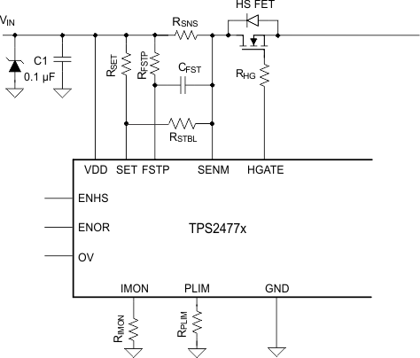 Figure 19. Adding RSTBL for VSNS,CL > 67.5mV
10.2.3.2 Selecting the Fast Trip Threshold and Filtering
The TPS2477x allows the user to program the fast trip threshold. When this threshold is exceeded the gate is quickly pulled down (<1µs). In addition CFSTP can be added to include some filtering into the comparator. The selection of the fast trip threshold and filtering is influenced by the systems environment and requirements. In general, picking a larger threshold and larger filtering time will result in more immunity to nuisance trips, but also a slower response (possibly inadequate) to real fault conditions. It’s best to fine tune these threshold after testing the real system. As a starting point it is recommended to set the fast trip threshold at least 1.25x larger than then current limit. For this design example a 150A fast trip threshold along with a 500ns filtering time constant were targeted to ensure that the transient requirement will be passed. The value for RFSTP and CFSTP can be computed as shown below:


The next closest standard resistor and capacitor values should be chosen. In this case RFSTP = 249Ω and CFSTP=2nF
10.2.3.3 Selecting the Hot Swap FET(s)
It is critical to select the correct MOSFET for a Hot Swap design. The device must meet the following requirements:
- The VDS rating should be sufficient to handle the maximum system voltage along with any ringing caused by transients. For most 12V systems a 25 V or 30V FET is a good choice.
- The SOA of the FET should be sufficient to handle all usage cases: start-up, hot-short, start into short.
- RDSON should be sufficiently low to maintain the junction and case temperature below the maximum rating of the FET. In fact, it is recommended to keep the steady state FET temperature below 125°C to allow margin to handle transients.
- Maximum continuous current rating should be above the maximum load current and the pulsed drain current must be greater than the current threshold of the circuit breaker. Most MOSFETs that pass the first three requirements will also pass these two.
- A VGS rating of +16 V is required, because the TPS2477x can pull up the gate as high as 15.5 V above source.
For this design the CSD16415Q5B was selected for its low RDSON and superior SOA. After selecting the MOSFET, the maximum steady state case temperature can be computed as follows:

In the equation above n is the number of FETs used in parallel. For this example 4 FETS are used in parallel to prevent over- heating and improve efficiency. Note that the RDSON is a strong function of junction temperature, which for most MOSFETS will be very close to the case temperature. A few iterations of the above equations may be necessary to converge on the final RDSON and TC,MAX value. According to the CSD16415Q5B datasheet, its RDSON is about 1.3x greater at 100°C compared to room temperature . The equation below uses this RDSON value to compute the TC,MAX. Note that the computed TC,MAX is close to the junction temperature assumed for RDSON. Thus no further iterations are necessary. For this example an RθCA of 50°C/W was used since there are 4 FETs close together and it’s expected that they will heat each other up. It’s highly recommended to test the board at full load and double check the thermals with the calculations.

10.2.3.4 Select Power Limit
In general, a lower power limit setting is preferred to reduce the stress on the MOSFET. However, at low power limit levels both the VSNS and VIMON become very low, which results in more error caused by offsets. It is recommended to keep VSNS above 1.5mV and VIMON above 27mV to ensure reasonable accuracy of the power limit engine. Based on these requirements the minimum power limit can be computed as shown below.

In most applications the power limit can be set to PLIM,MIN using the equation below. Here RSNS and RPWR are in Ωs and PLIM is in Watts.

The closest available resistor should be selected. In this case it is a 118 kΩ.
10.2.3.5 Set Fault Timer
The inrush timer runs when the Hot Swap is in power limit or current limit, which is the case during start-up. Thus the timer has to be sized large enough to prevent a time-out during start-up. If the part starts directly into current limit (ILIM x VDS < PLIM) the maximum start time can be computed with the equation below:

For most designs (including this example) ILIM,CL x VDS > PLIM so the Hot Swap will start in power limit and transition into current limit. In that case the maximum start time can be computed as follows:

Note that the above start-time is based on typical current limit and power limit values. To ensure that the timer never times out during start-up it is recommended to set the fault time (TINR) to be 1.5x tstart,max or 6 ms. This will account for the variation in power limit, timer current, and timer capacitance.
Next the designer should decide if having equal TINR and TFLT is acceptable. Note that to pass the load transient the fault timer needs to be longer than 200 ms. If the inrush time is this long, it will place too much stress on the MOSFET during a start into short. For this reason, it’s ideal to have two separate timers. To ensure proper start up and to pass the load transient a target inrush time (TINR,TGT) of 6 ms and a target fault time (TFLT,TGT) of 250ms is used. CINR,CLC and CFLT,CLC is computed as follows:


The next largest available CINR is chosen as 47 nF and the next largest available CFLT is chosen as 2.2µF
Next, the actual TINR and TFLT can be computed as shown below: Once the CTMR is chosen the actual programmed time out can be computed as follows.


10.2.3.6 Check MOSFET SOA
Once the power limit and fault timer are chosen, it’s critical to check that the FET will stay within its SOA during all test conditions. For this design example the TPS24772 is used, which does not retry during a hot-short. Thus the worst condition is a start-up into a short circuit. In this case the TPS24772 will start into a power limit and regulate at that point for 6.2 ms (TINR). Based on the SOA of the CSD16415Q5B, it can handle 13 V, 15 A for 10 ms and it can handle 13 V, 100 A for 1 ms. The SOA for 6.2 ms can be extrapolated by approximating SOA vs time as a power function as shown below:
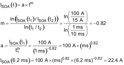
Note that the SOA of a MOSFET is specified at a case temperature of 25°C, while the case temperature can be hotter during a start into a short. It is important to understand the hottest temperature that a MOSFET can be during a start-up (TC, MAX, START). If a board has been off for a while and then it’s turned on TA, MAX is a good estimate for TC,MAX, START. However, if a board is on and then gets power cycled or a hot board is unplugged and plugged back in TC,MAX should be used for TC,MAX,START. This will depend on system requirements. For this design example it’s assumed that the board can only be plugged in cold and TA,MAX is used to estimate TC,MAX,START.

Based on this calculation the MOSFET can handle 17 A, 13 V for 6.2 ms at 55°C elevated case temperature, but is only required to handle 9A during a start into short. Thus there is good margin and this will be a robust design. In general, it is recommended that the MOSFET can handle 1.3x more than what is required during a hot-short. This provides margin to cover the variance of the power limit and fault time.
10.2.3.7 Choose Under Voltage and Over Voltage Settings
The TPS2477x has comparators with 1.35V threshold on the ENHS, ENOR, and OV pins. A resistor divider can be used to set Undervoltage and Overvoltage thresholds for the bus. For this design example 10V and 14V were chosen as the limits to allow some margin for the 11V to 13V input bus. Once these limits are known, RDIV2 and RDIV3 can be computed using the equations below. RDIV1 was set to 49.9 kΩ, which keeps the power consumption reasonable low without being too susceptible to leakage currents.


Choose closest available resistors standard 1% resistors: RDIV2 = 2.21 kΩ and RDIV3 = 5.62 kΩ. The actual Under Voltage and Over Voltage settings can be computed for the chosen resistors as follows:


10.2.3.8 Selecting C1 and COUT
It is recommended to add ceramic bypass capacitors to help stabilize the voltages on the input and output. Since CIN will be charged directly on hot-plug, its value should be kept small. 0.1µF is a good target. Since COUT doesn’t get charged during hot-plug, a larger value such as 1 µF could be used.
10.2.3.9 Adding CENHS
When the ENHS pin is pulled below its threshold and raised back up the IC will reset. Note that during a hot short the input voltage can easily droop below the UV threshold and cycle the ENHS pin. For the TPS24770 and TPS24771 ICs this will not change the behavior. However, when using the TPS24772 the cycling of the ENHS will result in the IC attempting to restart, which is undesired (this is the main reason why someone would use the TPS24772). To avoid this behavior a capacitor should be added to the ENHS to provide filtering. 33 nF was chosen for this example.
10.2.3.10 Selecting D1 and D2
During hot plug and hot short events there could be significant transients on the input and output of the Hot Swap that could cause operation outside of the IC specifications. To ensure reliable operation a TVS on the input and a Schottkey diode on the output are recommended. In this example a SMDJ14A and MBRS330T3G are used.
10.2.3.11 Checking Stability
For most applications, the TPS2477x is stable without any additional components. However in some cases additional CGS,EXT is required as shown in the following figure to help stabilize the current and power limit loop. Typically this is for low current limits and low sense voltages. It is easy to check whether these extra components are needed using the equations below. Note that the transconductance (also referred to as gm and gfs) of the FET will vary based on the current and thus gm' is used in the equations as a normalizing parameter. The CSD16415Q5B has a gm of 168 siemens at 40A of IDS, resulting in gm' of 26.56. For this example, CGS,MIN (per FET) was computed to be 0.25nF, while the CISS of the CSD16415Q5B is 3.15nF providing plenty of margin for the design. In general it is recommended to have a 2x margin from the typical CISS and CGS,MIN to account for any variation that the FET would have. If the CISS of the MOSFET isn't large enough an external RC should be added as shown in the figure below.


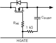 Figure 20. Adding CGS,EXT to Ensure Stability
10.2.3.12 Compute Tolerances
After finishing a design it is often desired to know the variations of each setting. Often times there are multiple error sources and there are two common ways to analyze the circuit. One is worst case, which adds all of the error sources and the other one is root sum square (RSS), which is less conservative. When error sources are independent, using the RSS method provides a more statistically accurate view of the tolerances. This method is used in this section. Note that the error calculations are quite long and tedious and it’s recommended to use TI’s excel tools, which support both worst case and RSS analysis. For this example the below tolerances are assumed. The following table lists the assumptions for the component tolerances. Note that the sense resistor itself is 1% accurate, but multiple two terminal 2512 resistors are used so additional error is introduced from solder resistance and layout limitations of paralleling resistors. For this example 3% is assumed as the total error of the sensing network.
Table 2. Component Tolerances
| COMPONENTS | TOLERANCE |
|---|---|
| RIMON and RSET | 1% |
| RSNS(Including Layout + Soldering) | 3% |
| RDIV1, RDIV2, RDIV3, RPLIM, RFST | 1% |
| CINR, CFLT | 10% |
First, the tolerance of the current monitoring and current limit is computed.
There are 5 error sourcing contributing to the current monitoring accuracy on the IMON pin: tolerance of RSET (ERSET), tolerance of RIMON (ERIMON), tolerance of RSNS (ERSNS), the IC gain error (ERGAIN), and the IC offset error (EROS). All of these errors are in % with the exception of the offset error. To get a percent error due to the offset error (EROS%) simply divide the offset by the sense voltage. For the TPS2477x, ERGAIN is 0.4%, and EROS is 150 µV.
Based on these values the full scale (IFS,ERR,IMON) current monitoring accuracy at the Imon pin can be computed with the following equations.

Note that the TPS2477x detects the current limit when the IMON pin exceeds 675 mV. Thus the current limit error ILIM,ER is a combination of the IFS,ERR,IMON and the current limit error at the IMON pin (ILIM,ERR,IMON). The 675 mV threshold varies up to 15 mV so ILIM,ERR,IMON is 2.3% and the current limit error can be computed as follows:

Next the power limit error is computed. This error is made up of three sources: the error from external components (ERCOMP), the error when translating the sense voltage to IMON (IPL,ERR, IMON), and the error of the power limit engine at IMON (ERIMON,PL). Both ERSNS and ERIMON, PL are a function of the operating point of the power limit engine. Note that this error is greatest at largest VDS, since VSNS,PL is smallest (refer to Figure 12). For this example VDS is largest when VIN = 13 V (maximum VIN) and VOUT = 0 V and the error is computed at this operating point. The sense voltage (VSNS) and the voltage at the IMON pin (VIMON) should be computed for this operating point using the equations below:


The IPL,ERR,IMON can be computed similarly to IFS,ERR,IMON using the equation below.

The tolerance of the power limit engine is specified at three VIMON points in the datasheet: 135 mV (±20.3 mV), 67.5 mV (±10.1 mV), and 27 mV (±8.1 mV). To get the % error at the real operating point, the absolute error should be extrapolated and divided by VIMON as shown in the equation below. This is graphically depicted in Figure 23.

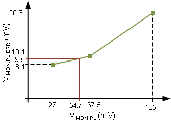 Figure 21. Extrapolating Power Limit Error
Once ERIMON,PL and IPL,ERR,IMON are known the total power limit error (PLERR,TOT) can be computed using the equation below. The component error (3.5%) comes from RSNS (3%), RPLIM (1%), RSET (1%), and RIMON (1%).

After computing the fast trip voltage threshold to be 24.9 mV (100 µA × 249 Ω), the fast trip threshold error resulting from the IC (FSTERR, IC) can be computed using a similar extrapolation method as used for power limit. The component error of RSNS and RFST should be added to obtain the total fast trip error (FSTERR,TOT). Both equations are shown below.


The IC error of the UV / OV threshold is always 3.7% (0.05 V / 1.35 V). Assuming that all resistors have a 1% error the component error is 1.41% (2 resistors). When using the RSS method the total error is 4%. For the timer error, the IC contributes 22% and 10% comes from the component. When using the RSS method the total error becomes 24.2%.
The table below summarizes the final tolerances of the design:
Table 3. Design Tolerances
| SETTINGS | ACCURACY |
|---|---|
| Current Limit | 4.1% |
| Fast Trip | 9.4% |
| Power Limit | 20.3% |
| TFLT, TINR | 24.2% |
| UV/OV | 4.0% |
10.2.4 Application Curves
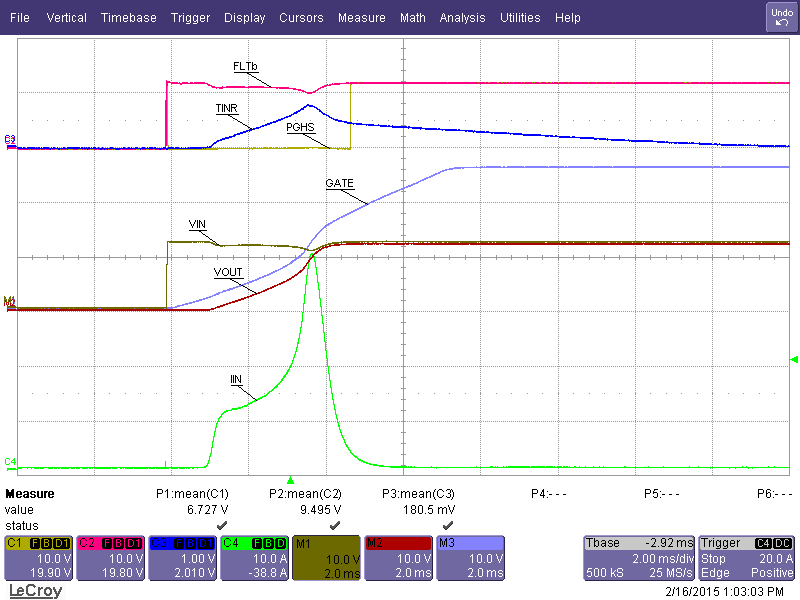 Figure 22. Start up (COUT=5500µF)
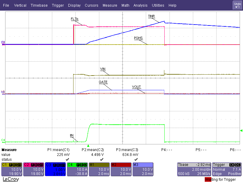 Figure 24. Start Up with Output Shorted to GND
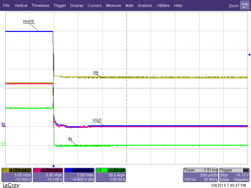 Figure 26. Hot Short on Output with Full Load
 (zoomed out)
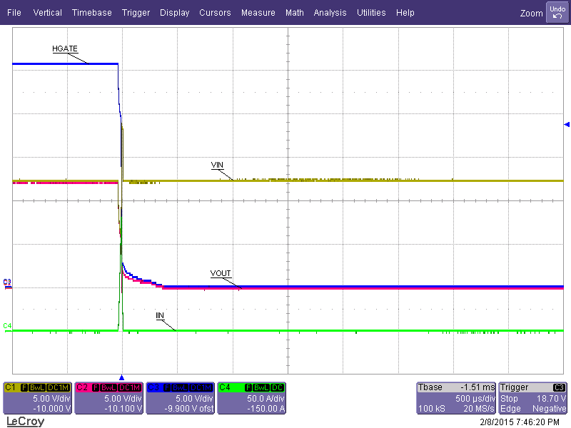 Figure 28. Hot Short on Output with No Load (zoomed out)
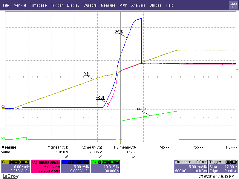 Figure 23. Undervoltage and Overvoltage
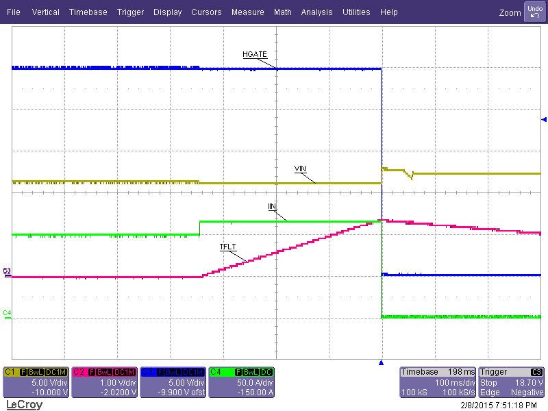 Figure 25. Load Step 100A to 120A
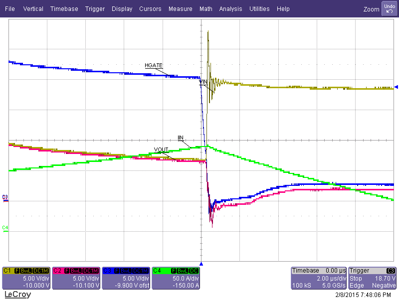 Figure 27. Hot Short on Output with Full Load
 (zoomed in)
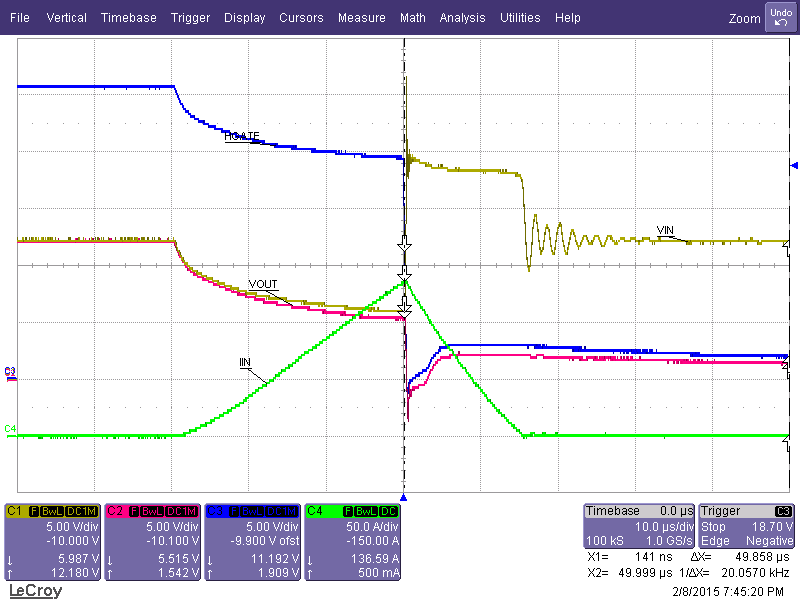 Figure 29. Hot Short on Output with No Load (zoomed in)
10.2.5 240 VA Application Using CSD16415Q5B
The diagram below shows the application schematic for this design example. See the TPS24770 Design Calculator to help with these calculations.
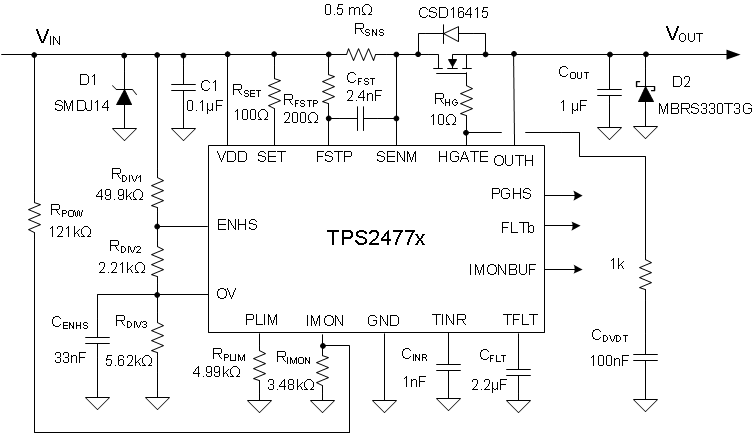 Figure 30. Application Schematic for 240VA Design with CSD16415Q5B
10.2.5.1 Design Requirements
The following table summarizes the requirements for this design. Note that the output power cannot exceed 240W for more than 250 ms.
Table 4. Design Requirements for a 240 VA Design using CSD16415Q5B
| DESIGN PARAMETER | EXAMPLE VALUE |
|---|---|
| Input voltage range | 10.8 V – 13.2V |
| Output Power Limit (VA limiting) | 240 W |
| Maximum Output Capacitance of the Hot Swap | 2500 uF |
| Maximum Ambient Temperature | 55°C |
| MOSFET RθCA (function of layout) | 35°C/W |
| Transient load requirement? | POUT is allowed to surpass 240W for <250 ms |
| Pass “Hot-Short” on Output? | Yes |
| Pass a “Start into short”? | Yes |
| Is the load off until PG asserted? | Yes |
| IC used | TPS24772 |
| Analog Current Monitor Used | No |
| MOSFET | CSD16415Q5B |
| Can a Hot Board be plugged in or Power Cycled? | Yes |
10.2.5.2 Theory of Operations
Before going into the details of the design it’s important to understand the impact that RPOW has on the circuit. Refer to Figure 31 for this discussion.
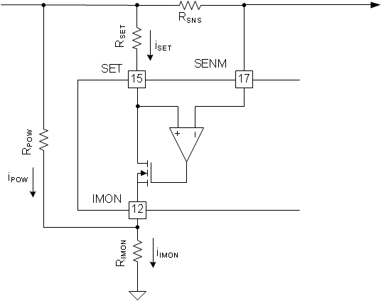 Figure 31. Impact of RPOW Resistor
Note that the TPS2477x detects overcurrent conditions when VIMON reaches 675mV, which occurs when there is sufficient current (iIMON) flowing through RIMON. Also note that iIMON is a sum of iSET and iPOW. If iIMON,CL, iSET,CL, and iPOW,CL correspond to these same current when VIMON reaches 675mV and TPS2477x detects current limit, the following equations can be written.


Also note that the amplifier ensures that SET and SENM are equal and thus ILIM can be derived as follows:


Examining the equation above, it can be seen that ILIM reduces as VIN becomes larger. Note that the ultimate goal is to limit output power. However, when the FET is on, VIN is very close to VOUT and they can be assumed to be equal.
The figure below compares the ideal ILIM vs VOUT (ILIM =240 W / VOUT) profile to that of the RPOW implementation shown here. The error is large when the output voltage is far from 12V, but the performance is quite good near 12V. The next figure shows the effective output power limit for output voltages from 10 V to 14 V. It can be seen that the results are quite good and much better than using a simple 20A current limit, without the RPOW resistor to compensate for VIN variation.
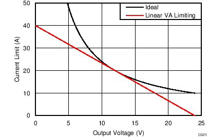 Figure 32. Current Limit (with RPOW) vs Output Voltage
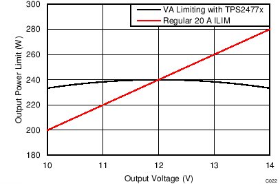 Figure 33. Output Power Limiting using RPOW vs Standard ILIM
10.2.5.3 Design Procedure
10.2.5.3.1 Select VSNS,CL, RSNS, and RSET Setting
For this example, VSNS,CL of 10 mV was selected to optimize efficiency. Then RSNS can be computed to 0.5mΩ. There is some flexibility in picking the RSET value. In this case targeting 100 µA for ISET,CL, RSET is computed to be 100 Ω as shown in the following equation.

10.2.5.3.1.1 Select RPOW and RIMON
RPOW controls the slope of the ILIM vs VIN curve and thus the ideal slope should be found first before selecting RPOW. This can be done by taking the derivative of the ideal current limit (ILIM, IDEAL) vs VIN curve and evaluating it at 12V. This is found to be –1.667 A/V as shown in the equations below. Next the derivative of equation 51 is taken to isolate the terms that influence the slope of ILIM vs VIN curve. Since RSET and RSNS have already been selected, RPOW remains the only parameter that can be varied. Thus, RPOW is computed using the last equation below.


The closest available standard resistor is chosen for RPOW, which is 121kΩ.
Next RIMON should be chosen to ensure that the output power limit is 240 W at 12 V, which is the typical operating point. RIMON is computed to be 3.49kΩ and the closest available standard resistor of 3.48 kΩ is chosen.


10.2.5.3.1.2 Selecting the Hot Swap FET(s)
It is critical to select the correct MOSFET for a Hot Swap design. The device must meet the following requirements:
- The VDS rating should be sufficient to handle the maximum system voltage along with any ringing caused by transients. For most 12V systems a 25 V or 30V FET is a good choice.
- The SOA of the FET should be sufficient to handle all usage cases: start-up, hot-short, start into short.
- RDSON should be sufficiently low to maintain the junction and case temperature below the maximum rating of the FET. In fact, it is recommended to keep the steady state FET temperature below 125°C to allow margin to handle transients.
- Maximum continuous current rating should be above the maximum load current and the pulsed drain current must be greater than the current threshold of the circuit breaker. Most MOSFETs that pass the first three requirements will also pass these two.
- A VGS rating of +16 V is required, because the TPS2477x can pull up the gate as high as 15.5 V above source.
For this design the CSD16415Q5B was selected for its low RDSON and superior SOA. After selecting the MOSFET, the maximum steady state case temperature can be computed as follows:

In the equation above n is the number of FETs used in parallel. Note that the RDSON is a strong function of junction temperature, which for most MOSFETS will be very close to the case temperature. A few iterations of the above equations may be necessary to converge on the final RDSON and TC,MAX value. According to the CSD16415Q5B datasheet, its RDSON is about 1.2 x greater at 75°C compared to room temperature. . The equation below uses this RDSON value to compute the TC,MAX. Note that the computed TC,MAX is close to the junction temperature assumed for RDSON. Thus no further iterations are necessary.

10.2.5.3.1.3 Keeping MOSFET within SOA During Normal Start-up
Next, the designer must ensure that the MOSFET will stay within SOA during start-up and a start-up into short. Note that the TPS24772 (fast latch off) is used for this design so the MOSFET stress during a hot short is minimal.
Since RPOW biases the IMON pin, it interferes with FET power limiting and it’s recommended to disable FET power limiting it by selecting a 4.99kΩ resistor for RPOW.
The inrush current can be limited by adding a capacitor from HGATE to GND (CDVDT) as shown in the application diagram. This capacitor limits the slew rate of HGATE at start-up, which will in turn limit the slew rate of VOUT. Assuming that the load is off until PGHS is asserted, all of the inrush current would be going into COUT and be inversely proportional to the slew rate of VOUT. Refer to the application plots for a start-up waveform. In addition, a 1kΩ resistor is placed in series with CDVDT to ensure that CDVDT doesn’t slow down the short circuit response of the Hot Swap.
For this example, a 100 nF capacitor was used for CDVDT. This results in an inrush current (IINR) of 1.375A, total inrush time (tINR) of 24.5, and peak FET power dissipation (PFET,PEAK) of 18.7W as shown in equations below. This assumes maximum input voltage of 13.2 V


Next, it’s importation to check that the MOSFET can handle this stress level. Note that the power dissipation of the MOSFET will start at PINR,MAX and will reduce to zero as the VDS drop across the MOSFET reduces. The effective stress on the MOSFET can be approximated to be PINR,MAX for tINR/2, which is the equivalent amount of energy. For this example, the FET stress is 18.7W for 12.3 ms. Looking at the SOA curve of the CSD16415Q5B, at VDS of 13.2 V it can handle ~15A for 10ms or ~4A for 100ms. Using the same method as the previous design example, it can be computed that the MOSFET can handle 13.4A for 12.3 ms when VDS=13.2 V.
The SOA of a MOSFET is specified at a case temperature of 25°C, while the real case temperature can be hotter during a start into a short. It is important to understand the hottest temperature that a MOSFET can be during a start-up (TC, MAX, START). If a board has been off for a while and then it’s turned on, TA, MAX is a good estimate for TC,MAX, START. However, if a board is on and then gets power cycled or gets unplugged and plugged back in, TC,MAX should be used for TC,MAX,START. This will depend on system requirements. For this design example, it is assumed that a hot board can be power cycled or hot plugged and thus TC,MAX is used to estimate TC,MAX,START.

Based on this calculation the MOSFET can handle 8.4 A, 13.2 V for 12.3 ms at 72°C elevated case temperature, but is only required to handle 1.375 A. Thus there is good margin and this will be a robust design. In general a 1.3x margin is recommended to cover for variations.
Next, the start into short case is considered. Since the MOSFET power limit is disabled, the current through the MOSFET will reach 20A before the part starts to regulate and runs the inrush timer. In order to minimize FET stress, a short inrush timer is chosen (1nF of CINR). Unfortunately, when a very short timer is used and there is a dv/dt capacitor, the FET stress cannot be simply estimated by TINR. In the following figure, it is clear that the FET has both voltage and significant current across it for longer than just TINR. This occurs because TINR is only activated when IIN reaches the current limit threshold, which doesn’t happen immediately due to the slow dv/dt on the gate and the limited transconductance of the FET.
The current is not a square pulse, which makes it hard to compare the FET stress to the SOA curves. Thus the stress shown in the following figure needs to be converted to an equivalent square pulse. For this example, the equivalent pulse was assumed to be 20 A for 1ms. The MOSFET can handle 100A, 13.2 V for 1ms, which can be derated to 62 A when accounting for elevated case temperature. This provides plenty of margin and ensures a robust design.

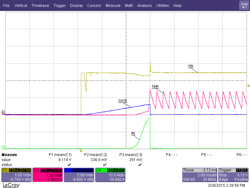 Figure 34. Start-up Into Short
10.2.5.3.1.4 Choose Fault Timer
To pass the load transient, a target fault time (TFLT,TGT) of 250ms is used. CFLT,CLC is computed as follows:

The next largest available CFLT is chosen as 2.2µF, which results in a TFLT of 290ms as shown below.

10.2.5.3.1.5 Choose Under Voltage and Over Voltage Settings
For this design example 10V and 14V were chosen as the limits to allow some margin for the 10.8V to 13.2V input bus. These are identical to the previous design example. See Choose Under Voltage and Over Voltage Settings section for programming these thresholds.
10.2.5.3.1.6 Selecting CIN and COUT
It is recommended to add ceramic bypass capacitors to help stabilize the voltages on the input and output. Since CIN will be charged directly on hot-plug, it’s value should be kept small. 0.1µF is a good target. Since COUT doesn’t get charged during hot-plug, a larger value such as 1 µF could be used.
10.2.5.3.1.7 Selecting D1 and D2
During hot plug and hot short events there could be significant transients on the input and output of the Hot Swap that could cause operation outside of the IC specifications. To ensure reliable operation a TVS on the input and a Schottkey diode on the output are recommended. In this example a SMDJ14A and MBRS330T3G are used.
10.2.5.3.1.8 Adding CENHS
When the ENHS pulled below its threshold and raised back up the IC will reset. Note that during a hot short the input voltage can easily droop below the UV threshold and cycle the ENHS pin. For the TPS24770 and TPS24771 ICs this will not change the behavior. However, when using the TPS24772 the cycling of the ENHS will result in the IC attempting to restart, which is undesired (this is the main reason why someone would use the TPS24772). To avoid this behavior a capacitor should be added to the ENHS to provide filtering. 33 nF was chosen for this example.
10.2.5.3.1.9 Stability Considerations
Since there is a 100nF CDVDT attached to HGATE, this significantly increases the effective capacitance of HGATE and guarantees stability for this application.
10.2.5.4 Application Curves
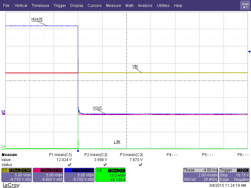 Figure 35. No Load then Hot Short (Zoomed Out)
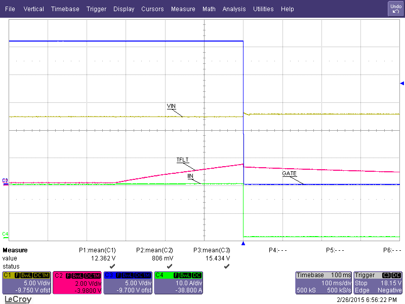 Figure 37. Overcurrent
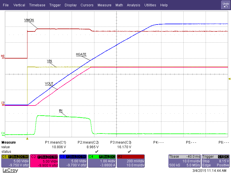 Figure 39. Start up (COUT = 2500 µF)
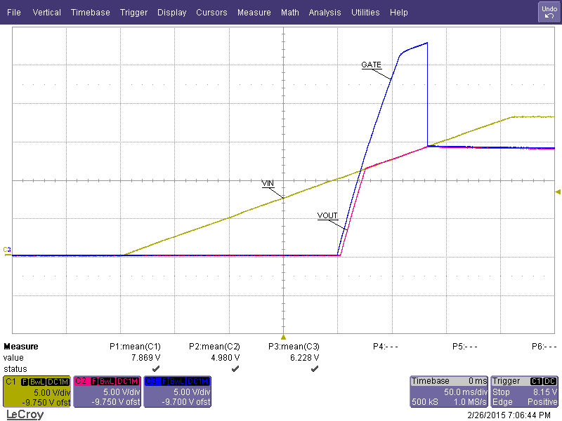 Figure 41. Under Voltage and Over Voltage with VIN Rising
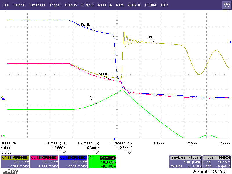 Figure 36. Full Load then Hot Short (Zoomed In)
 Figure 38. Start Up into Short
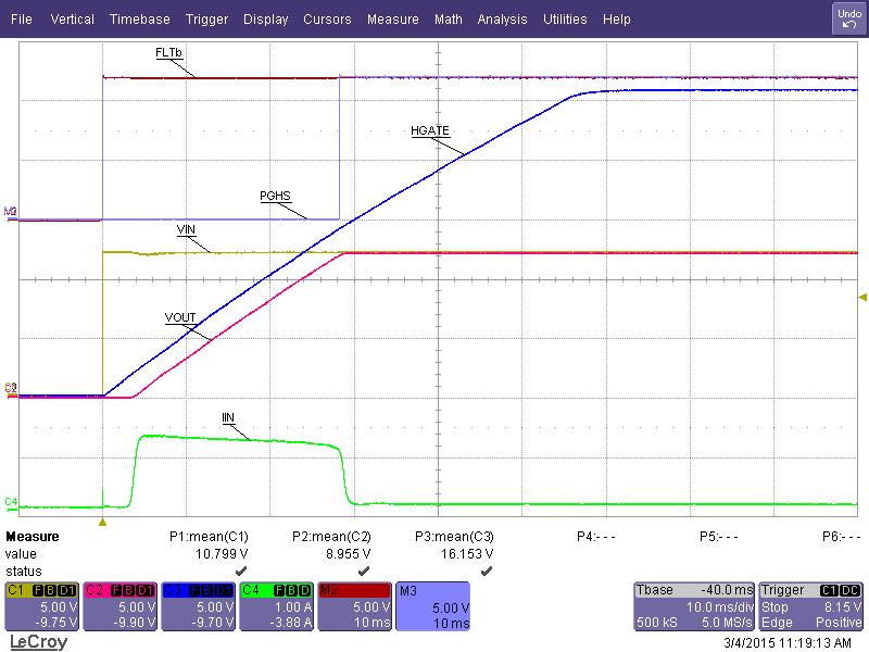 Figure 40. Start up showing PGHS and FLTb (COUT = 2500 µF)
10.2.6 240 VA Application Using CSD17573Q5B
This design example has identical requirements to the previous one, but the CSD17573Q5B is used instead of the CSD16415Q5B. The CSD17573Q5B is cheaper and offers better RDSON, but its SOA is not as good. Thus it was necessary to add Q2 and RSET2 to reduce the stress during a start up into a short circuit. Given that Q2 is a small signal PFET that is cheap, the overall BOM cost of this solution should be cheaper than the previous one. See the TPS24770 Design Calculator to help with these calculations.
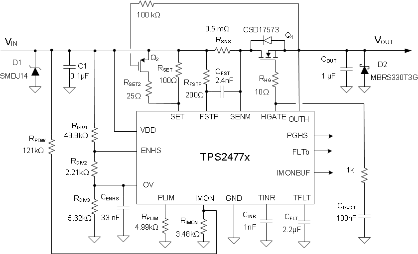 Figure 42. 240 VA Design Using CSD17573Q5B
10.2.6.1 Design Requirements
The following table summarizes the requirements for this design.
Table 5. Design Requirements for the 240 VA Design Using CSD17573Q5B
| DESIGN PARAMETER | EXAMPLE VALUE |
|---|---|
| Input voltage range | 10.8 V – 13.2 V |
| Output Power Limit (VA limiting) | 240 W |
| Maximum Output Capacitance of the Hot Swap | 2500 µF |
| Maximum Ambient Temperature | 55°C |
| MOSFET RθCA (function of layout) | 35°C/W |
| Transient load requirement? | POUT is allowed to surpass 240W for <250 ms |
| Pass “Hot-Short” on Output? | Yes |
| Pass a “Start into short”? | Yes |
| Is the load off until PG is asserted? | Yes |
| IC used | TPS24772 |
| Analog Current Monitor Used | No |
| MOSFET | CSD17573Q5B |
| Can a Hot Board be plugged in or Power Cycled? | Yes |
10.2.6.1.1 Choosing C1, COUT, CFLT, CENHS, D1, D2, RSET, RPOW, RIMON, RSNS, CDVDT, RPLIM, and UV/OV Thresholds
These components and settings are chosen in the same fashion as the previous design example. See 240 VA Application Using CSD16415Q5B.
10.2.6.1.2 Selecting the Hot Swap FET(s)
It is critical to select the correct MOSFET for a Hot Swap design. The device must meet the following requirements:
- The VDS rating should be sufficient to handle the maximum system voltage along with any ringing caused by transients. For most 12V systems a 25 V or 30V FET is a good choice.
- The SOA of the FET should be sufficient to handle all usage cases: start-up, hot-short, start into short.
- RDSON should be sufficiently low to maintain the junction and case temperature below the maximum rating of the FET. In fact, it is recommended to keep the steady state FET temperature below 125°C to allow margin to handle transients.
- Maximum continuous current rating should be above the maximum load current and the pulsed drain current must be greater than the current threshold of the circuit breaker. Most MOSFETs that pass the first three requirements will also pass these two.
- A VGS rating of +16 V is required, because the TPS2477x can pull up the gate as high as 15.5 V above source.
For this design the CSD17573Q5B was selected for its low RDSON and great cost point. After selecting the MOSFET, the maximum steady state case temperature can be computed as follows:

In the equation above n is the number of FETs used in parallel. Note that the RDSON is a strong function of junction temperature, which for most MOSFETS will be very close to the case temperature. A few iterations of the above equations may be necessary to converge on the final RDSON and TC,MAX value. According to the CSD17573Q5B datasheet, its RDSON is about 1.2 x greater at 65°C compared to room temperature. The equation below uses this RDSON value to compute the TC,MAX. Note that the computed TC,MAX is close to the junction temperature assumed for RDSON. Thus no further iterations are necessary.

10.2.6.1.3 Keeping the MOSFET within SOA
As in the previous example, it is important to ensure that the MOSFET stays within its SOA during both regular start-up and start-up into short.
First consider the regular start-up. The same CDVDT is used as the last example so the FET is required to handle 18.2W (or 1.38A and 13.2V) for 12.3 ms. Based on the SOA curve of the CSD17573Q55B, at VDS of 13.2 V it can handle 4.5 A for 10 ms or 2 A for 100 ms. Using the same method as the previous design example, it can be inferred that the MOSFET can handle 4.2 A for 12.3 ms when VDS=13.2 V.
The SOA of a MOSFET is specified at a case temperature of 25°C, while the case temperature can be hotter during a start into a short. It is important to understand the hottest temperature that a MOSFET can be during a start-up (TC, MAX, START). If a board has been off for a while and then it’s turned on TA, MAX is a good estimate for TC,MAX, START. However, if a board is on and then gets power cycled TC,MAX should be used for TC,MAX,START. This will depend on system requirements. For this design example, it’s assumed that a hot board can be power cycled or hot plugged and TC,MAX is used to estimate TC,MAX,START.

Based on this calculation the MOSFET can handle 2.7 A, 13.2 V for 12.3 ms at 69°C elevated case temperature, but is only required to handle 1.38 A. Thus there is sufficient margin to make this a robust design. Again a 1.3x margin is recommended to cover for variations.
Next, consider the start into short condition. Similar to the previous design the MOSFET would need to handle 20A and 13.2 V for ~1ms. Checking the SOA curve of the CSD17573Q5B, it can only handle 10A and 13.2 V for 1ms, so it’s SOA is clearly not sufficient.
This is where Q2 and RSET2 come in. They serve to reduce the current limit during starting up (ILIM,START) while the VDS of the Hot Swap MOSFET is above VT of Q2 (1V to 2V). The ratio of ILIM to ILIM,START, denoted as IRATIO, is a function of RSET and RSET2 as shown below. For this example a ratio of 0.2 (ILIM,START=4A) was targeted to reduce MOSFET stress, keep the current limit above IINR, and ensure sufficient signal on VSNS to keep the error reasonable. Once IRATIO is chosen, RSET2 is computed to be 25 Ω as shown below.


The start-up into short (with RSET2 and Q2) is shown in Figure 43 below. The equivalent power pulse is now 4A for ~0.5ms. The MOSFET can handle 10A, 13.2 V for 1ms, which can be derated to 6.5 A when accounting for elevated case temperature. Since the MOSFET is only required to handle 4A for 0.5ms there is plenty of margin in the design.

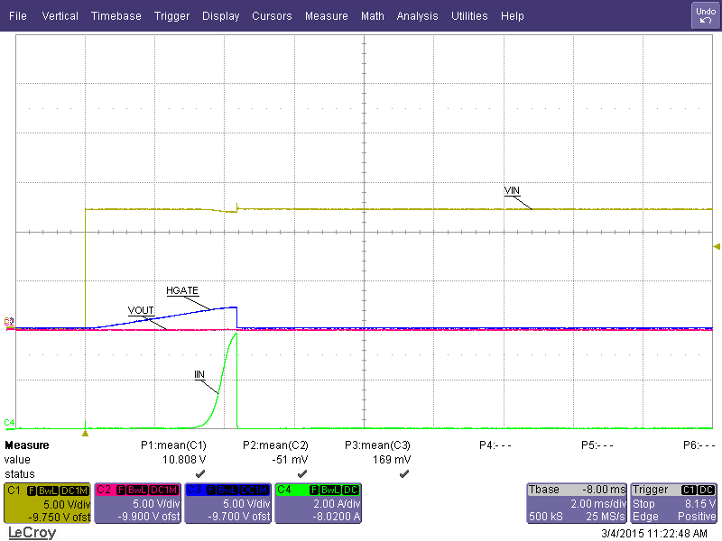 Figure 43. Start-up Into Short (with RSET and Q2)
10.2.6.2 Q2 Selection
There is a lot of flexibility when selecting Q2. Any PMOS with a ±20V VGS rating and 20V of VDS rating is sufficient. For this example IRLML5203PbF was used. Note that the 100k series resistor along with the CISS of Q2 (~500pF) for a filter with a 50 µs time constant. This protects Q2 in case there is high frequency ringing on VIN that causes VIN – VOUT to exceed 20V. This will usually happened during hot-plug or hot-short.
10.2.6.3 Application Curves
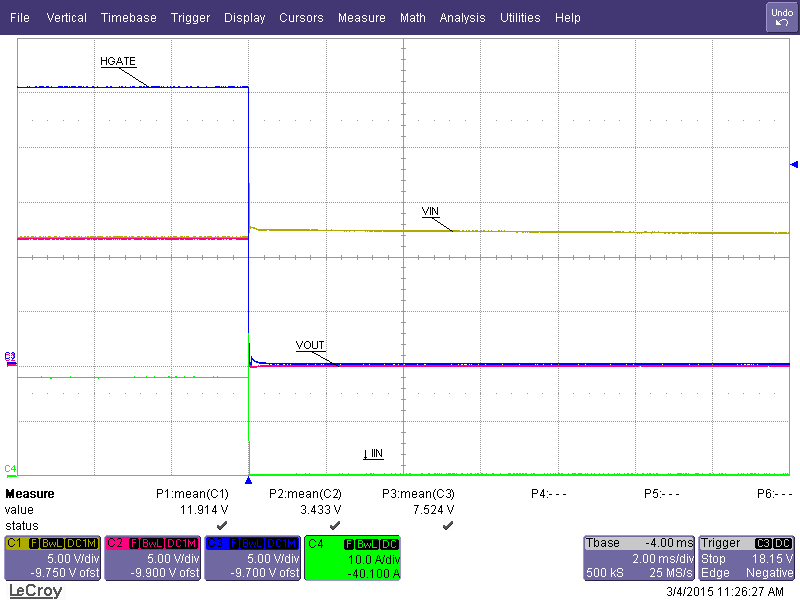 Figure 44. Full Load then Hot Short (Zoomed Out)
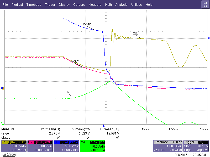 Figure 45. Full Load then Hot Short (Zoomed In)
 Figure 46. Over Current
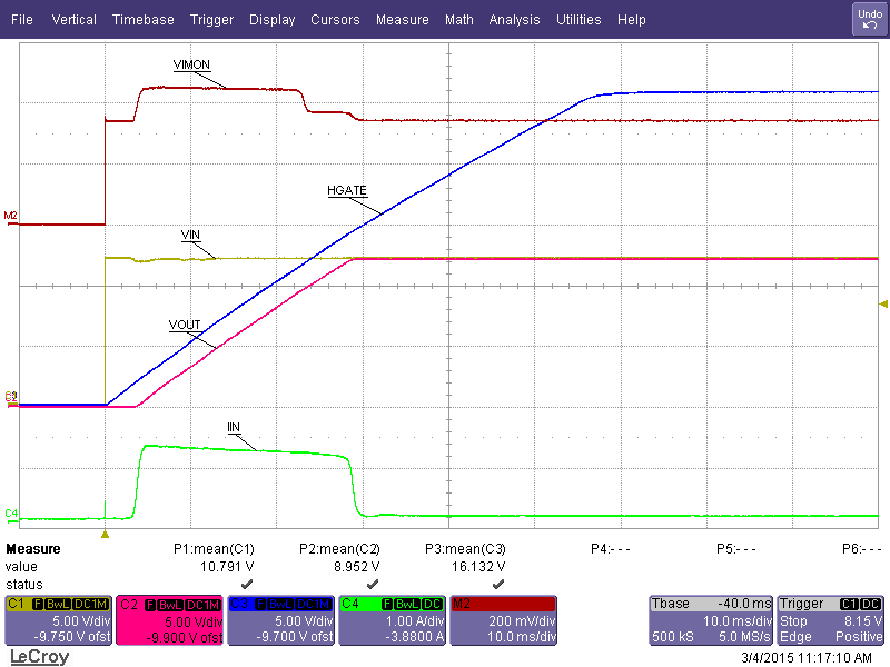 Figure 48. Start up (COUT = 2500 µF)
 Figure 50.
 Figure 47. Start Up Into Short
 Figure 49. Start up showing PGHS and FLTb (COUT = 2500 µF)