SLVSCZ3 March 2015 TPS24770 , TPS24771 , TPS24772
PRODUCTION DATA.
- 1 Features
- 2 Applications
- 3 Description
- 4 Simplified Schematic
- 5 Revision History
- 6 Device Comparison Table
- 7 Pin Configuration and Functions
- 8 Specifications
-
9 Detailed Description
- 9.1 Overview
- 9.2 Functional Block Diagram
- 9.3
Feature Description
- 9.3.1 Enable and Over-voltage Protection
- 9.3.2 Current Limit and Power Limit during Start-up
- 9.3.3 Two Level Protection During Regular Operation
- 9.3.4 Dual Timer (TFLT and TINR)
- 9.3.5 3 Options for Response to a Fast Trip
- 9.3.6 Using Soft Start - IHGATE and TINR Considerations
- 9.3.7 Analog Current Monitor
- 9.3.8 Power Good Flag
- 9.3.9 Fault Reporting
- 9.4 Device Functional Modes
-
10Application and Implementation
- 10.1 Application Information
- 10.2
Typical Application
- 10.2.1 12 V, 100 A, 5,500 µF Analog Hot Swap Design
- 10.2.2 Design Requirements
- 10.2.3
Detailed Design Procedure
- 10.2.3.1 Select RSNS and VSNS,CL Setting
- 10.2.3.2 Selecting the Fast Trip Threshold and Filtering
- 10.2.3.3 Selecting the Hot Swap FET(s)
- 10.2.3.4 Select Power Limit
- 10.2.3.5 Set Fault Timer
- 10.2.3.6 Check MOSFET SOA
- 10.2.3.7 Choose Under Voltage and Over Voltage Settings
- 10.2.3.8 Selecting C1 and COUT
- 10.2.3.9 Adding CENHS
- 10.2.3.10 Selecting D1 and D2
- 10.2.3.11 Checking Stability
- 10.2.3.12 Compute Tolerances
- 10.2.4 Application Curves
- 10.2.5
240 VA Application Using CSD16415Q5B
- 10.2.5.1 Design Requirements
- 10.2.5.2 Theory of Operations
- 10.2.5.3
Design Procedure
- 10.2.5.3.1
Select VSNS,CL, RSNS, and RSET Setting
- 10.2.5.3.1.1 Select RPOW and RIMON
- 10.2.5.3.1.2 Selecting the Hot Swap FET(s)
- 10.2.5.3.1.3 Keeping MOSFET within SOA During Normal Start-up
- 10.2.5.3.1.4 Choose Fault Timer
- 10.2.5.3.1.5 Choose Under Voltage and Over Voltage Settings
- 10.2.5.3.1.6 Selecting CIN and COUT
- 10.2.5.3.1.7 Selecting D1 and D2
- 10.2.5.3.1.8 Adding CENHS
- 10.2.5.3.1.9 Stability Considerations
- 10.2.5.3.1
Select VSNS,CL, RSNS, and RSET Setting
- 10.2.5.4 Application Curves
- 10.2.6 240 VA Application Using CSD17573Q5B
- 11Power Supply Recommendations
- 12Layout
- 13Device and Documentation Support
- 14Mechanical, Packaging, and Orderable Information
パッケージ・オプション
メカニカル・データ(パッケージ|ピン)
- RGE|24
サーマルパッド・メカニカル・データ
- RGE|24
発注情報
12 Layout
12.1 Layout Guidelines
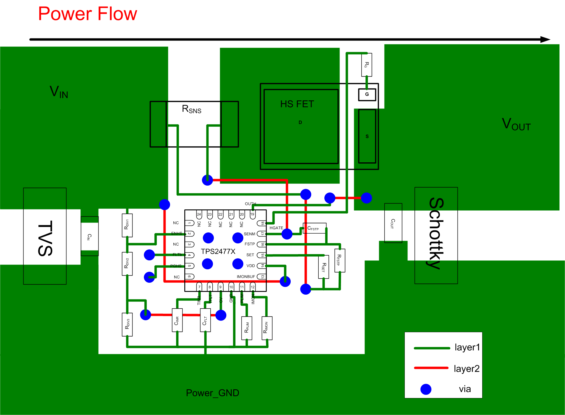
When doing the layout of the TPS2477x the following are considered best practice.
- Ensure proper Kelvin Sense of RSNS.
- Keep the filtering capacitor CFSTP as close to the IC as possible.
- Place a Shottky diode and a ceramic bypass capacitor close to the source of the Hot Swap MOSFET
- Do not connect VDD to the Kelvin Sense trace for SET and FSTP
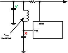
- Note that special care must be taken when placing the bypass capacitor for the VDD pin. During Hot Shorts, there is a very large dv/dt on input voltage during the MOSFET turn off. If the bypass capacitor is placed right next to the pin and the trace from RSNS to the pin is long, an LC filter is formed. As a result a large differential voltage can develop between VDD and SENM if there is a large transient on Vin. This could result in a violation of the abs max rating from VDD to SENM. To avoid this, place the bypass capacitor close to RSNS instead of the VDD pin.
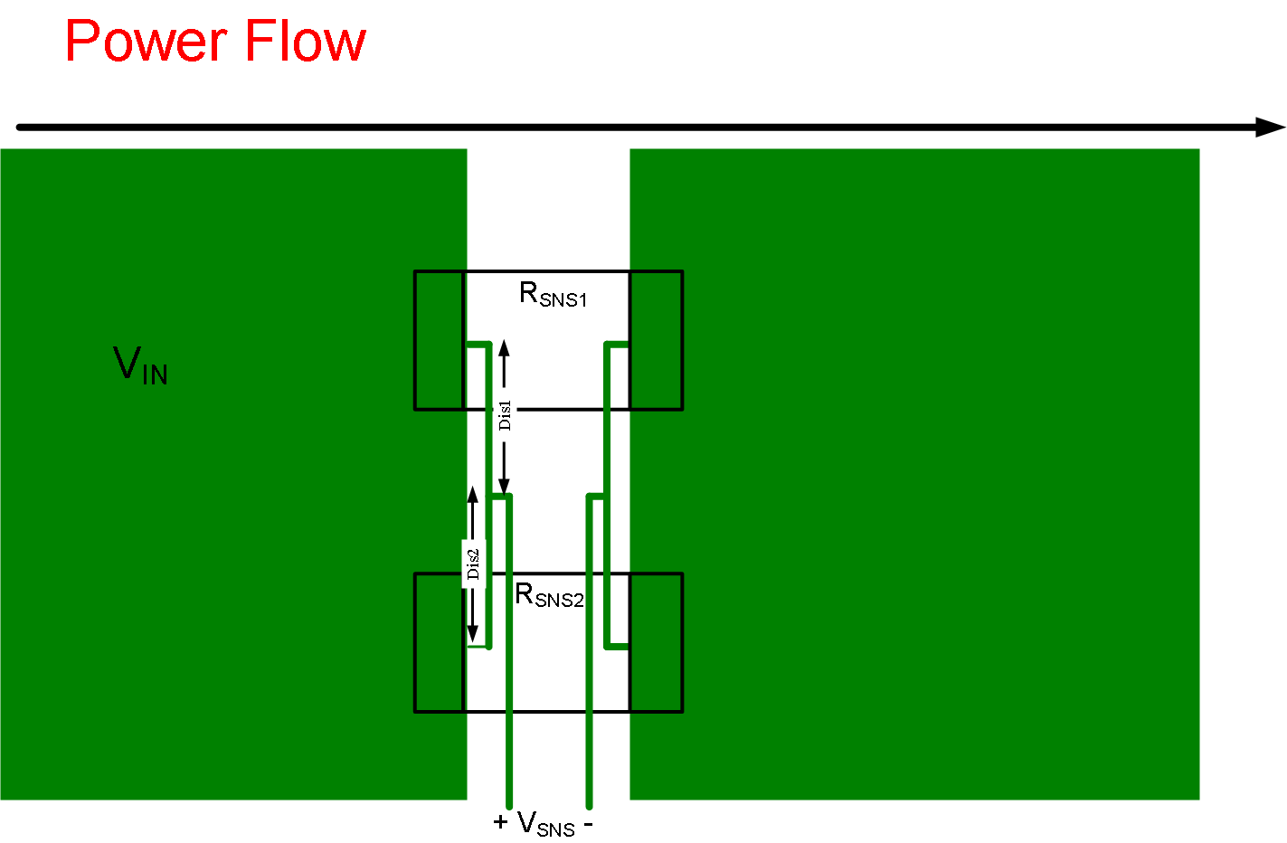
- When using parallel resistors the layout becomes even more critical. Due to PCB parasitics, the current through each RSNS may be different, which results in different sense voltages across the two resistors. It’s important to average these in order to get a proper current measurement. This can be accomplished by forming a resistor divider with the traces. As long as Dis1 = Dis2, the final VSNS will be an average of the drop across the two resistors.
 Figure 51. Layout Don't
 Figure 52. Sense Layout with 2 RSNS
12.2 Layout Example
