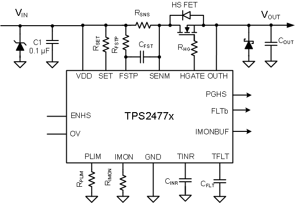
The TPS2477x is a high performance analog Hot Swap Controller for 2.5 V to 18 V systems. The precise and highly programmable protection settings of the TPS2477x aid the design of high power high availability systems where isolating faults is critical.
Programmable current limit, fast shut down, and fault timer protect the load and supply during fault conditions such as a hot - short. The fast shutdown threshold and response time can be tuned to ensure a fast response to real faults, while avoiding nuisance trips. Programmable Safe Operating Area (SOA) protection and the inrush timer keep the MOSFET safe under all conditions. After asserting power good, TPS2477x acts as a circuit breaker and runs the fault timer during over current events, but doesn’t current limit. It shuts down after the fault timer expires. Two independent timers (inrush/fault) allow the user to customize protection based on system requirements.
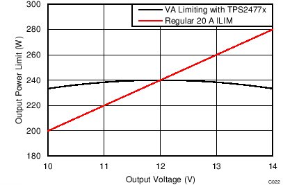
Finally, the flexibility of the TPS2477x aid Hot Swap design for the 240 VA requirement and a design example is shown in the datasheet.
PART NUMBER | PACKAGE | BODY SIZE (NOM) |
---|---|---|
TPS24770 TPS24771 TPS24772 |
RGE (24) | 4.00 mm x 4.00 mm |
DATE | REVISION | NOTES |
---|---|---|
March 2015 | * | Initial release. |
PART NUMBER(1) | LATCH / RETRY OPTION |
---|---|
TPS24770 | Latch |
TPS24771 | Auto – Retry |
TPS24772 | Fast Latch Off |
PIN | TYPE(1) | DESCRIPTION | |
---|---|---|---|
NAME | NO. | ||
ENHS | 2 | I | Active-high enable input of Hot Swap. Logic input. Connects to resistor divider. |
FLTb | 4 | O | Active-low, open-drain output indicating various faults. |
FSTP | 16 | I | Fast trip programming set pin for Hot Swap. A resistor is connected from positive terminal of RSNS to FSTP. |
GND | 10 | – | Ground. |
HGATE | 18 | O | Gate driver output for external Hot Swap MOSFET. |
IMON | 12 | I/O | Analog monitor and current limit program point. Connect RIMON to ground. |
IMONBUF | 13 | O | Voltage output proportional to the load current (0V–3.0V). |
NC | 1,3, 6, 20–24 | NC | No connect. Tie to ground or leave floating. |
OUTH | 19 | I | Output voltage sensor for monitoring Hot Swap MOSFET's power. Connects to the source terminal of the Hot Swap N channel MOSFET. |
OV | 9 | I | Overvoltage comparator input. Connects to resistor divider. HGATE is pulled low when OV exceeds the threshold. Connect to ground when not used. |
PGHS | 5 | O | Active-high, open-drain power-good indicator. |
PLIM | 11 | I | Power limit programming pin. A resistor from this pin to GND sets the maximum power dissipation for the Hot Swap FET. Connect a 4.99 kΩ resistor to disable power limit. |
SENM | 17 | I | Current-sensing input for the sense resistor. Directly connects to the negative terminal of the sense resistor. |
SET | 15 | I | Current-limit programming set pin for Hot Swap. A resistor is connected from positive terminal of the sensing resistor. |
TFLT | 8 | I/O | Fault timer, which runs when the device is in regular operation and there is an overcurrent condition. |
TINR | 7 | I/O | Inrush timer, which runs during the inrush operation (start-up) if the part is in current limit or power limit. |
VDD | 14 | P | Power Supply |
MIN | MAX | UNIT | ||
---|---|---|---|---|
Input Voltage | VDD,SET, FSTP,SENM, OUTH, ENHS, FLTb, PGHS, OV | –0.3 | 30 | V |
HGATE to OUTH | –0.3 | 15 | V | |
SET to VDD | –0.3 | 0.3 | V | |
SENM, FSTP to VDD | –0.6 | 0.3 | V | |
TINR, TFLT, PLIM, IMON | –0.3 | 3.6 | V | |
IMONBUF | –0.3 | 7 | V | |
Sink Current | FLTb, PGHS | 5 | mA | |
Source Current | IMON, IMONBUF | 5 | mA | |
Storage temperature, Tstg | –65 | 150 | °C |
VALUE | UNIT | |||
---|---|---|---|---|
V(ESD)(1) | Electrostatic discharge | Human-body model (HBM), per ANSI/ESDA/JEDEC JS-001(2) | ±1500 | V |
Charged-device model (CDM), per JEDEC specification JESD22-C101(3) | ±500 |
MIN | MAX | UNIT | ||
---|---|---|---|---|
Input voltage | VDD, SENM, SET, FSTP | 2.5 | 18 | V |
ENHS, FLTb, PGHS, OUTH | 0 | 18 | ||
Sink current | FLTb, PGHS | 0 | 2 | mA |
Source current | IMON | 0 | 1 | mA |
External resistance | PLIM | 4.99 | 500 | kΩ |
IMON | 1 | 6 | kΩ | |
FSTP | 10 | 4000 | Ω | |
SET | 10 | 400 | Ω | |
RIMON / RSET | w/o RSTBL | 10 | 70 | |
With appropriate RSTBL(1) | 3 | 10 | ||
with CHGATE > 47nF (2) | 10 | 200 | ||
External capacitor | TINR, TFLT | 1 | nF | |
HGATE, (2) | 0 | 1 | µF | |
IMON | 30 | pF | ||
IMONBUF | 100 | pF | ||
Operating junction temperature, TJ | –40 | 125 | °C |
THERMAL METRIC(1) | RGE | UNIT | |
---|---|---|---|
24 PINS | |||
RθJA | Junction-to-ambient thermal resistance | 34.6 | °C/W |
RθJC(top) | Junction-to-case (top) thermal resistance | 38.4 | |
RθJB | Junction-to-board thermal resistance | 12.9 | |
ψJT | Junction-to-top characterization parameter | 0.5 | |
ψJB | Junction-to-board characterization parameter | 12.9 | |
RθJC(bot) | Junction-to-case (bottom) thermal resistance | 3.2 |
PARAMETER | TEST CONDITION | MIN | TYP | MAX | UNIT | |
---|---|---|---|---|---|---|
INPUT SUPPLY (VDD) | ||||||
VUVR | UVLO threshold, rising | 2.2 | 2.32 | 2.45 | V | |
VUVhyst | UVLO hysteresis | 0.10 | V | |||
IQON | Supply current: IVDD + IOUTH | Device on, VENHS = 2V | 2.95 | 4 | mA | |
Hot Swap FET ENABLE (ENHS) | ||||||
VENHS | Threshold voltage, rising | 1.3 | 1.35 | 1.4 | V | |
VENHShyst | Hysteresis | 50 | mV | |||
IENHS | Input Leakage Current | 0 ≤ VENHS ≤ 30V | –1 | 1 | µA | |
OVER VOLTAGE (OV) | ||||||
VOVR | Threshold voltage, rising | 1.3 | 1.35 | 1.4 | mV | |
VOVhyst | Hysteresis | 50 | mV | |||
IOV | Input leakage current | 0 ≤ VOV ≤ 30V | –1 | 1 | µA | |
POWER LIMIT PROGRAMING (PLIM) | ||||||
VPLIM,BIAS | Bias voltage | Sourcing 10μA | 0.65 | 0.675 | 0.7 | V |
VIMON,PL | Regulated IMON voltage during power limit | RPLIM = 52 kΩ; VSENM-OUTH=12V | 114.75 | 135 | 155.25 | mV |
RPLIM = 105 kΩ; VSENM-OUTH=12V | 56.95 | 67 | 77.05 | |||
RPLIM = 261 kΩ; VSENM-OUTH=12V | 18.9 | 27 | 35.1 | |||
RPLIM = 105 kΩ; VSENM-OUTH=2V | 341.7 | 402 | 462.3 | |||
RPLIM = 105 kΩ; VSENM-OUTH=18V | 38.25 | 45 | 51.75 | |||
SLOW TRIP THRESHOLD (SET) | ||||||
VOS_SET | Input referred offset (VSNS to VIMON scaling) | RSET = 44.2Ω; RIMON=3kΩ to 1.2kΩ (VSNS,CL=10mV to 25mV) | –150 | 150 | µV | |
VGE_SET | Gain error (VSNS to VIMON scaling)(1) | –0.4% | 0.4% | |||
FAST TRIP THRESHOLD PROGRAMMING (FSTP) | ||||||
IFSTP | FSTP input bias current | VFSTP=12V | 95 | 100 | 105 | µA |
VFASTRIP | Fast trip threshold | RFSTP = 200 Ω, VSNS when VHGATE ↓ | 18 | 20 | 22 | mV |
RFSTP = 1 kΩ, VSNS when VHGATE ↓ | 95 | 100 | 105 | |||
RFSTP = 4 kΩ, VSNS when VHGATE ↓ | 380 | 400 | 420 | |||
CURRENT SUMMING NODE (IMON) | ||||||
VIMON,CL | Slow trip threshold at summing node | VIMON↑, when ITFLT starts sourcing | 660 | 675 | 690 | mV |
IIMON-LKG | IMON leakage current | VENHS =0V, VIMON = 1.5V | –200 | 200 | nA | |
CURRENT MONITOR (IMONBUF) | ||||||
VOS_IMONBUF | Buffer offset | VIMON = 50mV to 675mV, Input referred | –3 | 0 | 3 | mV |
GAINIMONBUF | Buffer voltage gain | ΔVIMONBUF / ΔVIMON | 2.97 | 2.99 | 3.01 | V |
BWIMONBUF | Buffer closed loop bandwidth | CIMONBUF = 75pF | 1 | MHz | ||
Hot Swap GATE DRIVER (HGATE) | ||||||
VHGATE | HGATE output voltage | 5 ≤ VVDD ≤ 16V; measure VHGATE-OUTH | 12 | 13.6 | 15.5 | V |
2.5V <VVDD < 5V; 16V <VVDD < 20V measure VHGATE-OUTH |
7 | 7.95 | 15 | V | ||
VHGATEmax | Clamp voltage | Inject 10μA into HGATE, measure V(HGATE – OUTH) | 12 | 13.9 | 15.5 | V |
IHGATEsrc | Sourcing current | VHGAT-OUTH = 2V-10V | 44 | 55 | 66 | µA |
IHGATEfastSink | Sinking current for fast trip | VHGATE-OUTH = 2V–15V; V(FSTP – SENM) = 20mV | 0.45 | 1 | 1.6 | A |
IHGATEsustSink | Sustained sinking current | Sustained, VHGATE-OUTH = 2V – 15V; VENHS = 0 | 30 | 44 | 60 | mA |
INRUSH TIMER (TINR) | ||||||
ITINRsrc | Sourcing current | VTINR = 0V, In power limit or current limit | 8 | 10.25 | 12.5 | µA |
ITINRsink | Sinking current | VTINR = 2V, In regular operation | 1.5 | 2 | 2.5 | µA |
VTINRup | Upper threshold voltage | Raise VTINR until HGATE starts sinking | 1.3 | 1.35 | 1.4 | V |
VTINRlr | Lower threshold voltage | Raise VTINR to 2V. Reduce VTINR until ITINR is sourcing. | 0.33 | 0.35 | 0.37 | v |
RTINR | Bleed down resistance | VVDD = 0V, VTINR = 2V | 70 | 104 | 130 | kΩ |
ITINR-PD | Pulldown current | VTINR = 2V, when VENHS = 0V | 2 | 4.2 | 7 | mA |
RETRYCYCLE | Cycle number | # of timer cycles before retry (TPS24771 only) | 64 | 64 | 64 | |
RETRYDUTY | Retry duty cycle | TFLT and TINR connected (TPS24771 only) | 0.70% | |||
TFLT and TINR not connected (TPS24771 only) | 0.35% | |||||
VIMON,TINR | See Using Soft Start - IHGATE and TINR Considerations | RPLIM = 52kΩ, VSENM = 12V, VOUTH = 0 V. Raise IMON voltage and record IMON when TINR starts sourcing current. | 47.75 | 90 | 132.25 | mV |
VIMON,PL | See Using Soft Start - IHGATE and TINR Considerations | RPLIM = 52kΩ, VSENM-OUTH = 12V, Raise IMON voltage and record IMON when IHGATE starts sinking current. | 114.75 | 135 | 155.25 | mV |
ΔVIMON,TINR | See Using Soft Start - IHGATE and TINR Considerations | ΔVIMON,TINR = VIMON,PL - VIMON,TINR | 23 | 45 | 67 | mV |
FAULT TIMER (TFLT) | ||||||
ITFLTsrc | Sourcing current | VTFLT = 0V, PGHS is high and in overcurrent | 8 | 10.25 | 12.5 | µA |
ITFLTsink | Sinking current | VTFLT = 2V, Not in overcurrent | 1.5 | 2 | 2.5 | µA |
VTFLTup | Upper threshold voltage | Raise VTFLT until HGATE starts sinking | 1.3 | 1.35 | 1.4 | V |
RTFLT | Bleed down resistance | VENHS = 0V, VTFLT = 2V | 70 | 104 | 130 | kΩ |
ITFLT-PD | Pulldown current | VTFLT = 2V, when VENHS = 0V | 2 | 5.6 | 7 | mA |
HOT SWAP OUTPUT (OUTH) | ||||||
IOUTH, BIAS | Input bias current | VOUTH = 12V | 30 | 70 | µA | |
FAULT INDICATOR (FLTb) | ||||||
VOL_FLTb | Output low voltage | Sinking 2 mA | 0.11 | 0.25 | V | |
IFLTb | Input leakage current | VFLTb = 0V, 30V | –1 | 0 | 1 | µA |
VHSFLT_IMON | VIMON threshold to detect Hot Swap FET short | VENHS = 0V, Measured VIMON ↑ to GND when FLTb ↓ | 88 | 101 | 115 | mV |
VHSFL_hyst | Hysteresis | 25 | mV | |||
HOT SWAP POWER GOOD OUTPUT (PGHS) | ||||||
VPGHSth | PGHS Threshold | Measure VSENM-OUTH ↓ when PGHS↑ | 170 | 270 | 375 | mV |
VPGHShyst | PGHS hysteresis | VSENM-OUTH ↑ | 80 | mV | ||
VOL_PGHS | PGHS Output low voltage | Sinking 2mA | 0.11 | 0.25 | V | |
IPGHS | PHGS Input leakage current | VPGHS=0V to 30V | –1 | 0 | 1 | µA |
THERMAL SHUTDOWN (OTSD) | ||||||
TOTSD | Thermal shutdown threshold | Temperature rising | 140 | °C | ||
TOTSD,HYST | Hysteresis | 10 | °C |
PARAMETER | TEST CONDITION | MIN | TYP | MAX | UNIT | |
---|---|---|---|---|---|---|
INPUT SUPPLY (VDD) | ||||||
DEGLUVLO | UVLO deglitch | Both rising and falling | 14 | µs | ||
HOT SWAP FET ENABLE (ENHS) | ||||||
DEGLENHS | Deglitch time | Both rising and falling | 2.2 | 3.8 | 5.5 | µs |
OVER VOLTAGE (OV) | ||||||
DEGLOV | Deglitch time | Both rising and falling | 2.2 | 3.9 | 5.7 | µs |
FAST TRIP (FSTP) | ||||||
tFastOffDly | Fast turn-off delay | V(FSTP – SENM) : –5mV to 5mV, CHGATE = 0 pF | 600 | ns | ||
V(FSTP – SENM) : -20mV to 20mV CHGATE = 0 pF | 300 | |||||
tFastOffDur | Strong pull down current duration | 53 | 63 | 73 | µs | |
INRUSH TIMER (TINR) | ||||||
NRETRY | Number of TINR cycles before retry | TPS24741 only | 64 | |||
RETRYDUTY | Retry duty cycle | TINR not connected to TFLT | 0.35% | |||
TINR connected to TFLT | 0.7% | |||||
FAULT INDICATOR (FLTb) | ||||||
tFLT_degl | Fault deglitch | Both rising and falling | 2.2 | 3.9 | 5.3 | ms |
HOT SWAP POWER GOOD OUTPUT (PGHS) | ||||||
tPGHSdegl | PGHS deglitch time | Rising | 0.7 | 1 | 1.3 | ms |
Falling | 7 | 8 | 9 |
Iq = IVDD+IOUTH |
IPGHS =2mA |
VHGATE-VOUTH=10V |
Sustained sink current |
VHGATE-OUTH=4V | ||
RPLIM =52kΩ | ||
TJ =25°C |
VIMON during Power Limiting |
VHGATE-VOUTH=2V |