SPAS093C December 2009 – September 2015 TPS2505
PRODUCTION DATA.
- 1 Features
- 2 Applications
- 3 Description
- 4 Revision History
- 5 Pin Configuration and Functions
-
6 Specifications
- 6.1 Absolute Maximum Ratings
- 6.2 ESD Ratings
- 6.3 Recommended Operating Conditions
- 6.4 Thermal Information
- 6.5 Electrical Characteristics (Shared Boost, LDO and USB)
- 6.6 Electrical Characteristics (Boost Only)
- 6.7 Electrical Characteristics (USB1/2 Only)
- 6.8 Electrical Characteristics (LDO and Reset Only)
- 6.9 Recommended External Components
- 6.10 Dissipation Ratings
- 6.11 Typical Characteristics
- 7 Parameter Measurement Information
-
8 Detailed Description
- 8.1 Overview
- 8.2 Functional Block Diagram
- 8.3
Feature Description
- 8.3.1 PGND
- 8.3.2 IN
- 8.3.3 EN
- 8.3.4 GND
- 8.3.5 ILIM1/2
- 8.3.6 RESET
- 8.3.7 LDOOUT
- 8.3.8 LDOIN
- 8.3.9 ENLDO
- 8.3.10 FAULT1/2
- 8.3.11 ENUSB1/2
- 8.3.12 USB1/2
- 8.3.13 AUX
- 8.3.14 SW
- 8.3.15 Thermal Pad
- 8.3.16 Boost Converter
- 8.3.17 USB Switches
- 8.3.18 3.3-V LDO
- 8.3.19 Reset Comparator
- 8.3.20 Thermal Shutdown
- 8.3.21 Component Recommendations
- 8.4 Device Functional Modes
-
9 Application and Implementation
- 9.1 Application Information
- 9.2
Typical Application
- 9.2.1 Design Requirements
- 9.2.2 Detailed Design Procedure
- 9.2.3 Application Curves
- 10Power Supply Recommendations
- 11Layout
- 12Device and Documentation Support
- 13Mechanical, Packaging, and Orderable Information
11 Layout
11.1 Layout Guidelines
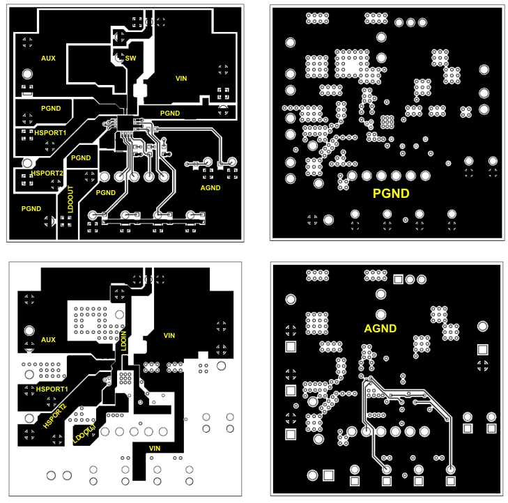
Layout is an important design step due to the high switching frequency of the boost converter. Careful attention must be applied to the PCB layout to ensure proper function of the device and to obtain the specified performance. Potential issues resulting from poor layout techniques include wider line and load regulation tolerances, EMI noise issues, stability problems, and USB current-limit shifts. It is critical to provide a low-impedance ground path that minimizes parasitic inductance. Wide and short traces should be used in the high-current paths, and components should be placed as close to the device as possible. Grounding is an important part of the layout. The device has a PGND and a GND pin. The GND pin is the quiet analog ground of the device and should have its own separate ground pour; connect the quiet signals to GND including the RILIM1/2 resistors and any input decoupling capacitors to the GND pour. It is important that the RILIM1/2 resistors be tied to a quiet ground to avoid unwanted shifts in the current-limit threshold. The PGND pin is the high-current power-stage ground; the ground pours of the output (AUX) and bulk input capacitors should be tied to PGND. PGND and GND should to be tied together in one location at the IC thermal pad, creating a star-point ground.
The output filter of the boost converter is also critical for layout. The inductor and AUX capacitors should be placed to minimize the area of current loop through AUX–PGND–SW.The layout for the TPS2505EVM evaluation board is shown in Figure 16 and should be followed as closely as possible for best performance.
11.2 Layout Example
 Figure 16. Layout Recommendation for TPS2505 Application – 4 Layer Board