SLUSB18A JUNE 2012 – August 2016 TPS2511
PRODUCTION DATA.
- 1 Features
- 2 Applications
- 3 Description
- 4 Revision History
- 5 Pin Configuration and Functions
- 6 Specifications
-
7 Detailed Description
- 7.1 Overview
- 7.2 Functional Block Diagram
- 7.3
Feature Description
- 7.3.1 Overcurrent Protection
- 7.3.2 Current Limit Threshold
- 7.3.3 Current-Sensing Report (CS)
- 7.3.4 Undervoltage Lockout (UVLO) and Enable (EN)
- 7.3.5 Soft Start, Reverse Blocking, and Discharge Output
- 7.3.6 Thermal Sense
- 7.3.7 VBUS Voltage Drop Compensation
- 7.3.8 Divide Mode Selection of 5-W and 10-W USB Chargers
- 7.4 Device Functional Modes
- 8 Application and Implementation
- 9 Power Supply Recommendations
- 10Layout
- 11Device and Documentation Support
- 12Mechanical, Packaging, and Orderable Information
パッケージ・オプション
メカニカル・データ(パッケージ|ピン)
- DGN|8
サーマルパッド・メカニカル・データ
- DGN|8
発注情報
10 Layout
10.1 Layout Guidelines
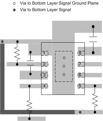
- TPS2511 placement. Place the TPS2511 near the USB output connector and at least 22-µF OUT pin filter capacitor. Connect the exposed PowerPAD to the GND pin and to the system ground plane using a via array.
- IN pin bypass capacitance. Place the 0.1-µF bypass capacitor near the IN pin and make the connection using a low-inductance trace.
- ILIM_SET pin connection. Current limit setpoint accuracy can be compromised by stray leakage from a higher voltage source to the ILIM_SET pin. Ensure that there is adequate spacing between IN pin copper or trace and ILIM_SET pin trace to prevent contaminant buildup during the PCB assembly process. The traces routing the RILIM resistor to the device must be as short as possible to reduce parasitic effects on the current limit accuracy.
- DP and DM consideration. Route these traces as differential micro-strips. For DP and DM, there is no internal IEC ESD cell, refer to application note Effective System ESD Protection Guidelines:TPS251x USB Charging Port Controllers for these 2 pins' IEC ESD design guideline.
10.2 Layout Example
For the trace routing of DP and DM, no strictly request must route these traces as micro-strips with nominal differential impedance of 90 Ω because no USB 2.0 high-speed data transmission on these data line. But because there is no internal IEC ESD cell, TI recommends placing IEC ESD cell on DP and DM trace close to USB connector.
 Figure 33. Layout Recommendation