JAJSCJ7 September 2016 TPS2549
PRODUCTION DATA.
- 1 特長
- 2 アプリケーション
- 3 概要
- 4 改訂履歴
- 5 Pin Configuration and Functions
- 6 Specifications
- 7 Parameter Measurement Information
-
8 Detailed Description
- 8.1 Overview
- 8.2 Functional Block Diagram
- 8.3 Feature Description
- 8.4 Device Functional Modes
- 9 Application and Implementation
- 10Power Supply Recommendations
- 11Layout
- 12デバイスおよびドキュメントのサポート
- 13メカニカル、パッケージ、および注文情報
8 Detailed Description
8.1 Overview
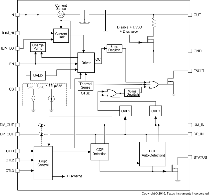
The TPS2549 device is a USB charging controller and power switch which integrates D+ and D– short to VBUS protection, cable compensation and IEC ESD protection, and is suitable for USB charging and USB port-protection applications.
The TPS2549 device integrates a current-limited, power-distribution switch using N-channel MOSFETs for applications where short circuits or heavy capacitive loads can be encountered. The device allows the user to program the current-limit threshold via an external resistor. The device enters constant-current mode when the load exceeds the current limit threshold.
The TPS2549 device also integrates CDP mode, defined in the BC1.2 specification, to enable up to 1.5-A fast charging of most of portable devices, meanwhile supporting data communication. In addition, the device integrates the DCP-auto feature to enable fast-charging of most portable devices including pads, tablets, and smart phones.
The TPS2549 device integrates a cable compensation (CS) feature to compensate the voltage drop in long cables and keep the remote USB port output voltage constant.
Additionally, the device integrates an IEC ESD cell to provide ESD protection up to ±8 kV (contact discharge) and ±15 kV (air discharge) per IEC 61000-4-2 on DP_IN and DM_IN, and integrates short-to-VBUS overvoltage protection on DP_IN and DM_IN to protect the upstream USB transceiver.
8.2 Functional Block Diagram
8.3 Feature Description
8.3.1 FAULT Response
The device features an active-low, open-drain fault output. FAULT goes low when there is a fault condition. Fault detection includes overtemperature, overcurrent, or DP_IN, DM_IN overvoltage. Connect a 10-kΩ pullup resistor from FAULT to IN.
Table 1 summarizes the conditions that generate a fault and actions taken by the device.
Table 1. Fault Conditions
| EVENT | CONDITION | ACTION |
|---|---|---|
| Overcurrent on V(OUT) | I(OUT) > IOS | The device regulates switch current at IOS until thermal cycling occurs. The fault indicator asserts and de-asserts with an 8-ms deglitch (The device does not assert FAULT on overcurrent in SDP1 and DCP1 modes). |
| Overvoltage on the data lines | DP_IN or DM_IN > 3.9 V | The device immediately shuts off the USB data switches. The fault indicator asserts with a 16-ms deglitch, and de-asserts without deglitch. |
| Overtemperature | TJ > OTSD2 in non-current-limited or TJ > OTSD1 in current-limited mode. |
The device immediately shuts off the internal power switch and the USB data switches. The fault indicator asserts immediately when the junction temperature exceeds OTSD2 or OTSD1 while in a current-limiting condition. The device has a thermal hysteresis of 20°C. |
8.3.2 Cable Compensation
When a load draws current through a long or thin wire, there is an IR drop that reduces the voltage delivered to the load. In the vehicle from the voltage regulator 5-V output to the VPD_IN (input voltage of portable device), the total resistance of power switch rDS(on) and cable resistance causes an IR drop at the PD input.. So the charging current of most portable devices is less than their expected maximum charging current.
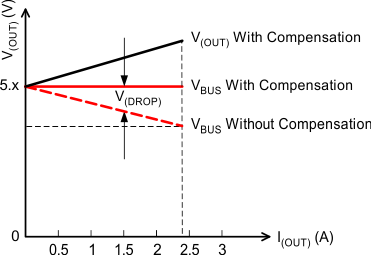 Figure 37. Voltage Drop
TPS2549 device detects the load current and generates a proportional sink current that can be used to adjust output voltage of the upstream regulator to compensate the IR drop in the charging path. The gain G(CS) of the sink current proportional to load current is 75 µA/A.
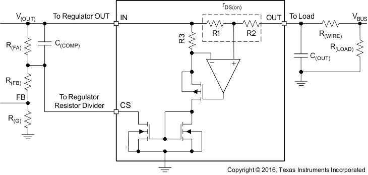 Figure 38. Cable Compensation Equivalent Circuit
8.3.2.1 Design Procedure
To start the procedure, the total resistance, including power switch rDS(on) and wire resistance R(WIRE), must to be known.
- Choose R(G) following the voltage-regulator feedback resistor-divider design guideline.
- Calculate R(FA) according to Equation 1.
- Calculate R(FB) according to Equation 2.
- C(COMP) in parallel with R(FA) is needed to stablilize V(OUT) when C(OUT) is large. Start with C(COMP) ≥ 3 × G(CS) × C(OUT), then adjust C(COMP) to optimize the load transient of the voltage regulator output. V(OUT) stability should always be verified in the end application circuit.


8.3.3 D+ and D– Protection
D+ and D– protection consists of ESD and OVP (overvoltage protection). The DP_IN and DM_IN pins integrate an IEC ESD cell to provide ESD protection up to ±15 kV air discharge and ±8 kV contact discharge per IEC 61000-4-2 (See the ESD Ratings section for test conditions). Overvoltage protection (OVP) is provided for short-to-VBUS conditions in the vehicle harness to prevent damaging the upstream USB transceiver. Short-to-GND protection for D+ and D– is provided by the upstream USB transceiver.
The ESD stress seen at DP_IN and DM_IN is impacted by many external factors like the parasitic resistance and inductance between ESD test points and the DP_IN and DM_IN pins. For air discharge, the temperature and humidity of the environment can cause some difference, so the IEC performance should always be verified in the end-application circuit.
8.3.4 Output and D+ or D– Discharge
To allow a charging port to renegotiate current with a portable device, the TPS2549 device uses the OUT discharge function. This function turns off the power switch while discharging OUT with a 500-Ω resistance, then turns the power switches to back on reassert the OUT voltage.
For DP_IN and DM_IN, when OVP is triggered, the device turns on an internal discharge path with 210-Ω resistance. On removal of OVP, this path can discharge the remnant charges to automatically turn on analog switch and turn off this discharge path, thus back into normal mode.
8.3.5 Port Power Management (PPM)
PPM is the intelligent and dynamic allocation of power. PPM is for systems that have multiple charging ports but cannot power them all simultaneously.
8.3.5.1 Benefits of PPM
The benefits of PPM include the following:
- Delivers better user experience
- Prevents overloading of system power supply
- Allows for dynamic power limits based on system state
- Allows every port to potentially be a high-power charging port
- Allows for smaller power-supply capacity because loading is controlled
8.3.5.2 PPM Details
All ports are allowed to broadcast high-current charging. The current-limit is based on ILIM_HI. The system monitors the STATUS pin to see when high-current loads are present. Once the allowed number of ports asserts STATUS, the remaining ports are toggled to a non-charging port. The non-charging port current-limit is based on the ILIM_LO setting. The non-charging ports are automatically toggled back to charging ports when a charging port de-asserts STATUS.
STATUS asserts in a charging port when the load current is above ILIM_LO + 40 mA for 210 ms (typical). STATUS de-asserts in a charging-port when the load current is below ILIM_LO – 10 mA for 3 seconds (typical).
8.3.5.3 Implementing PPM in a System With Two Charging Ports (CDP and SDP1)
Figure 39 shows the implementation of the two charging ports with data communication, each with a TPS2549 device and configured in CDP mode. In this example, the 5-V power supply for the two charging ports is rated at less than 3.5 A. Both TPS2549 devices have ILIM_LO of 1 A and ILIM_HI of 2.4 A. In this implementation, the system can support only one of the two ports at 2.4-A charging current, whereas the other port is set to SDP1 mode and I(LIMIT) corresponds to 1 A. In SDP1 mode, FAULT does not assert for overcurrent.
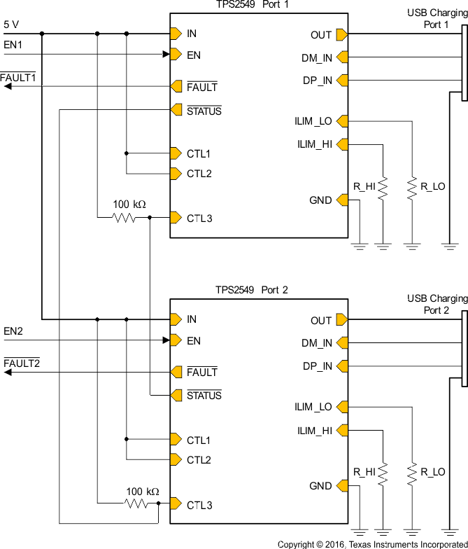 Figure 39. PPM With CDP and SDP1
8.3.5.4 Implementing PPM in a System With Two Charging Ports (DCP and DCP1)
Figure 40 shows the implementation of the two charging-only ports, each with a TPS2549 device and configured in DCP mode. In this example, the 5-V power supply for the two charging ports is rated at less than 3.5 A. Both TPS2549 devices have ILIM_LO of 1 A and ILIM_HI of 2.4 A. In this implementation, the system can support only one of the two ports at 2.4-A charging current, whereas the other port is set to DCP1 mode and I(LIMIT) corresponds to 1 A. In DCP1 mode, FAULT does not assert for overcurrent.
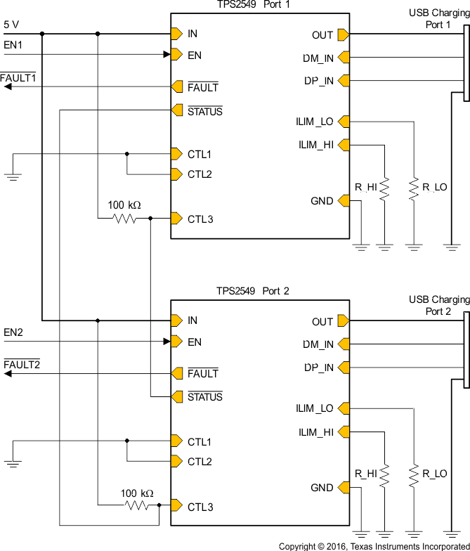 Figure 40. PPM With DCP and DCP1
8.3.6 CDP and SDP Auto Switch
The TPS2549 device is equipped with a CDP and SDP auto-switch feature to support some popular phones in the market. These popular phones do not comply with the BC1.2 specification because they fail to establish a data connection in CDP mode. These phones use primary detection (used to distinguish between an SDP and different types of charging ports) to only identify ports as SDP (data, no charge) or DCP (no data, charge). These phones do not recognize CDP (data, charge) ports. When connected to a CDP port, these phones classify the port as a DCP and only charge the battery. Because the charging ports are configured as CDP, users do not receive the expected data connection.
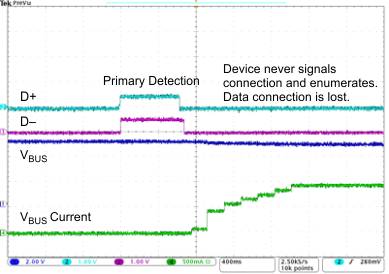 Figure 41. CDP and SDP Auto-Switch
To remedy this problem, the TPS2549 device employs a CDP and SDP auto-switch scheme to ensure these BC1.2 noncompliant phones establish data connection using the following steps.
- The TPS2549 device determines when a noncompliant phone has wrongly classified a CDP port as a DCP port and has not made a data connection.
- The TPS2549 device automatically completes an OUT (VBUS) discharge and reconfigures the port as an SDP.
- When reconfigured as an SDP, the phone detects a connection to an SDP and establishes a data connection.
- The TPS2549 device then switches automatically back to a CDP without doing an OUT (VBUS) discharge.
- The phone continues to operate as if connected to an SDP because OUT (VBUS) was not interrupted. The port is now ready in CDP if a new device is attached.
8.3.7 Overcurrent Protection
When an overcurrent condition is detected, the device maintains a constant output current and reduces the output voltage accordingly. Two possible overload conditions can occur. In the first condition, the output is shorted before the device enables or before the application of V(IN). The TPS2549 device senses the short and immediately switches into a constant-current output. In the second condition, a short or an overload occurs while the device is enabled. At the instant the overload occurs, high currents flow for 2 μs (typical) before the current-limit circuit reacts. The device operates in constant-current mode after the current-limit circuit has responded. Complete shutdown occurs only if the fault is presented long enough to activate overtemperature protection. The device remains off until the junction temperature cools to approximately 20°C and then restarts. The device continues to cycle on and off until the overcurrent condition is removed.
8.3.8 Undervoltage Lockout
The undervoltage-lockout (UVLO) circuit disables the device until the input voltage reaches the UVLO turnon threshold. Built-in hysteresis prevents unwanted oscillations on the output due to input voltage drop from large current surges.
8.3.9 Thermal Sensing
Two independent thermal-sensing circuits protect the TPS2549 device if the temperature exceeds recommended operating conditions. These circuits monitor the operating temperature of the power-distribution switch and disable operation. The device operates in constant-current mode during an overcurrent condition, which increases the voltage drop across power switch. The power dissipation in the package is proportional to the voltage drop across the power switch, so the junction temperature rises during an overcurrent condition. When the device is in a current-limiting condition, the first thermal sensor turns off the power switch when the die temperature exceeds OTSD1. If the device is not in a current-limiting condition, the second thermal sensor turns off the power switch when the die temperature exceeds OTSD2. Hysteresis is built into both thermal sensors, and the switch turns on after the device has cooled by approximately 20°C. The switch continues to cycle off and then on until the fault is removed. The open-drain false-reporting output, FAULT, is asserted (low) during an overtemperature shutdown condition.
8.3.10 Current Limit Setting
The TPS2549 has two independent current-limit settings that are each programmed externally with a resistor. The ILIM_HI setting is programmed with R(ILIM_HI) connected between ILIM_HI and GND. The ILIM_LO setting is programmed with R(ILIM_LO) connected between ILIM_LO and GND. Consult the device truth table (Table 2) to see when each current limit is used. Both settings have the same relation between the current limit and the programming resistor.
R(ILIM_LO) is optional and the ILIM_LO pin may be left unconnected if the following conditions are met:
- The TPS2549 device is configured as DCP(001) or CDP(111).
- Load detection is not used.
The following equation calculates the value of resistor for programming the typical current limit:

R(ILIM_xx) corresponds to either R(ILIM_HI) or R(ILIM_LO), as appropriate.
Many applications require that the current limit meet specific tolerance limits. When designing to these tolerance limits, both the tolerance of the TPS2549 current limit and the tolerance of the external programming resistor must be taken into account. The following equations approximate the TPS2549 minimum and maximum current limits to within a few milliamperes and are appropriate for design purposes. The equations do not constitute part of TI’s published device specifications for purposes of TI’s product warranty. These equations assume an ideal—no variation—external programming resistor. To take resistor tolerance into account, first determine the minimum and maximum resistor values based on its tolerance specifications and use these values in the equations. Because of the inverse relation between the current limit and the programming resistor, use the maximum resistor value in the I(OS_min) equation and the minimum resistor value in the I(OS_max) equation.


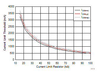
Resistor I
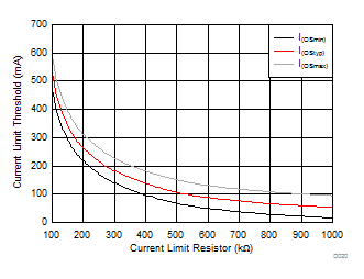
Resistor II
The routing of the traces to the R(ILIM_xx) resistors should have a sufficiently low resistance so as to not affect the current-limit accuracy. The ground connection for the R(ILIM_xx) resistors is also very important. The resistors must reference back to the TPS2549 GND pin. Follow normal board layout practices to ensure that current flow from other parts of the board does not impact the ground potential between the resistors and the TPS2549 GND pin.
8.4 Device Functional Modes
8.4.1 Device Truth Table (TT)
The device truth table (Table 2) lists all valid combinations for the three control pins (CTL1 through CTL3), and the corresponding charging mode of each pin combination. The TPS2549 device monitors the CTL inputs and transitions to whichever charging mode it is commanded to go to. For example, if the USB port is a charging-only port, then the user must set the CTL pins of the TPS2549 device to correspond to the DCP-auto charging mode. However, when the USB port requires data communication, then the user must set control pins to correspond to the SDP or CDP mode, and so on.
Table 2. Truth Table
| CTL1 | CTL2 | CTL3 | CURRENT LIMIT SETTING | MODE | STATUS OUTPUT (ACTIVE-LOW) | FAULT OUTPUT (ACTIVE-LOW) | CS FOR CABLE COMPENSATION | NOTES |
|---|---|---|---|---|---|---|---|---|
| 0 | 0 | 0 | Lo | DCP1(1) | OFF | ON(2) | ON | DCP includes divider 3, 1.2-V mode, and BC1.2 mode |
| 0 | 0 | 1 | Hi | DCP(1) | ON | ON | ON | DCP includes divider 3, 1.2-V mode, and BC1.2 mode |
| 0 | 1 | X | Lo | SDP | OFF | ON | ON | Standard SDP port |
| 1 | 0 | X | NA | Client mode | OFF | OFF | OFF | No current limit, power switch disabled, data switch bypassed |
| 1 | 1 | 0 | Lo | SDP1(3) | OFF | ON(2) | ON | Standard SDP port |
| 1 | 1 | 1 | Hi | CDP(3) | ON | ON | ON | CDP-SDP auto switch mode |
8.4.2 USB Specification Overview
The following overview references various industry standards. TI recommends consulting the most up-to-date standards to ensure the most recent and accurate information. Rechargeable portable equipment requires an external power source to charge batteries. USB ports are a convenient location for charging because of an available 5-V power source. Universally accepted standards are required to ensure host and client-side devices operate together in a system to ensure power-management requirements are met. Traditionally, host ports following the USB-2.0 specification must provide at least 500 mA to downstream client-side devices. Because multiple USB devices can be attached to a single USB port through a bus-powered hub, the client-side device sets the power allotment from the host to ensure the total current draw does not exceed 500 mA. In general, each USB device is granted 100 mA and can request more current in 100-mA unit steps up to 500 mA. The host grants or denies additional current based on the available current. A USB-3.0 host port not only provides higher data rate than a USB-2.0 port but also raises the unit load from 100 mA to 150 mA. Providing a minimum current of 900 mA to downstream client-side devices is required.
Additionally, the success of USB has made the micro-USB and mini-USB connectors a popular choice for wall-adapter cables. A micro-USB or mini-USB allows a portable device to charge from both a wall adapter and USB port with only one connector. As USB charging has gained popularity, the 500-mA minimum defined by USB 2.0, or 900 mA for USB 3.0, has become insufficient for many handset and personal media players, which require a higher charging rate. Wall adapters provide much more current than 500 or 900 mA. Several new standards have been introduced defining protocol handshaking methods that allow host and client devices to acknowledge and draw additional current beyond the 500-mA and 900-mA minimum defined by USB 2.0 and USB 3.0, respectively, while still using a single micro-USB or mini-USB input connector.
The TPS2549 device supports four of the most-common USB-charging schemes found in popular hand-held media and cellular devices.
- USB Battery Charging Specification BC1.2
- Chinese Telecommunications Industry Standard YD/T 1591-2009
- Divider 3 mode
- 1.2-V mode
The BC1.2 specification includes three different port types:
- Standard downstream port (SDP)
- Charging downstream port (CDP)
- Dedicated charging port (DCP)
BC1.2 defines a charging port as a downstream-facing USB port that provides power for charging portable equipment. Under this definition, CDP and DCP are defined as charging ports.
Table 3 lists the difference between these port types.
Table 3. Operating Modes Table
| PORT TYPE | SUPPORTS USB2.0 COMMUNICATION | MAXIMUM ALLOWABLE CURRENT DRAWN BY PORTABLE EQUIPMENT (A) |
|---|---|---|
| SDP (USB 2.0) | YES | 0.5 |
| SDP (USB 3.0) | YES | 0.9 |
| CDP | YES | 1.5 |
| DCP | NO | 1.5 |
8.4.3 Standard Downstream Port (SDP) Mode — USB 2.0 and USB 3.0
An SDP is a traditional USB port that follows USB 2.0 or USB 3.0 protocol. A USB 2.0 SDP supplies a minimum of 500 mA per port and supports USB 2.0 communications. A USB 3.0 SDP supplies a minimum of 900 mA per port and supports USB 3.0 communications. For both types, the host controller must be active to allow charging.
8.4.4 Charging Downstream Port (CDP) Mode
A CDP is a USB port that follows USB BC1.2 and supplies a minimum of 1.5 A per port. A CDP provides power and meets the USB 2.0 requirements for device enumeration. USB-2.0 communication is supported, and the host controller must be active to allow charging. The difference between CDP and SDP is the host-charge handshaking logic that identifies this port as a CDP. A CDP is identifiable by a compliant BC1.2 client device and allows for additional current draw by the client device.
The CDP handshaking process occurs in two steps. During step one, the portable equipment outputs a nominal 0.6-V output on the D+ line and reads the voltage input on the D– line. The portable device detects the connection to an SDP if the voltage is less than the nominal data-detect voltage of 0.3 V. The portable device detects the connection to a CDP if the D– voltage is greater than the nominal data detect voltage of 0.3 V and optionally less than 0.8 V.
The second step is necessary for portable equipment to determine whether the equipment is connected to a CDP or a DCP. The portable device outputs a nominal 0.6-V output on the D– line and reads the voltage input on the D+ line. The portable device concludes the equipment is connected to a CDP if the data line being read remains less than the nominal data detects voltage of 0.3 V. The portable device concludes it is connected to a DCP if the data line being read is greater than the nominal data detect voltage of 0.3 V.
8.4.5 Dedicated Charging Port (DCP) Mode
A DCP only provides power and does not support data connection to an upstream port. As shown in the following sections, a DCP is identified by the electrical characteristics of the data lines. The TPS2549 only emulates one state, DCP-auto state. In the DCP-auto state, the device charge-detection state machine is activated to selectively implement charging schemes involved with the shorted, divider3 and 1.2 v modes. The shorted DCP mode complies with BC1.2 and Chinese Telecommunications Industry Standard YD/T 1591-2009, whereas the divider3 and 1.2 V modes are employed to charge devices that do not comply with the BC1.2 DCP standard.
8.4.5.1 DCP BC1.2 and YD/T 1591-2009
Both standards specify that the D+ and D– data lines must be connected together with a maximum series impedance of 200 Ω, as shown in Figure 44.
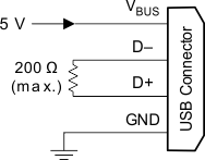 Figure 44. DCP Supporting BC1.2 and YD/T 1591-2009
8.4.5.2 DCP Divider-Charging Scheme
The device supports divider3, as shown in Figure 45. In the Divider3 charging scheme the device applies 2.7 V and 2.7 V to D+ and D– data lines.
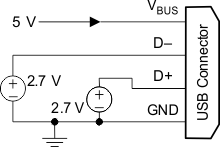 Figure 45. Divider 3 Mode
8.4.5.3 DCP 1.2-V Charging Scheme
The DCP 1.2-V charging scheme is used by some hand-held devices to enable fast charging at 2 A. The TPS2549 device supports this scheme in DCP-auto state before the device enters BC1.2 shorted mode. To simulate this charging scheme, the D+ and D– lines are shorted and pulled up to 1.2 V for a fixed duration. Then the device moves to DCP shorted mode as defined in the BC1.2 specification and as shown in Figure 46.
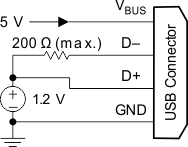 Figure 46. 1.2-V Mode
8.4.6 DCP Auto Mode
As previously discussed, the TPS2549 device integrates an auto-detect state machine that supports all the DCP charging schemes. The auto-detect state machine starts in the Divider3 scheme. However, if a BC1.2 or YD/T 1591-2009 compliant device is attached, the TPS2549 device responds by turning the power switch back on without output discharge and operating in 1.2-V mode briefly before entering BC1.2 DCP mode. Then the auto-detect state machine stays in that mode until the device releases the data line, in which case the auto-detect state machine goes back to the Divider3 scheme. When a Divider3-compliant device is attached, the TPS2549 device stays in the Divider3 state.
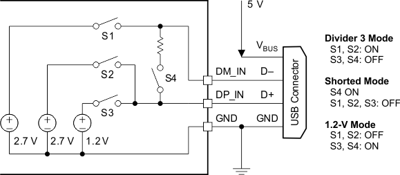 Figure 47. DCP Auto Mode
8.4.7 Client Mode
The TPS2549 device integrates client mode as shown in Figure 48. The internal power switch is OFF and only the data analog switch is ON to block OUT power. This mode can be used for some software programming via the USB port.
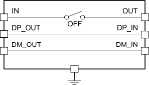 Figure 48. Client-Mode Equivalent Circuit
8.4.8 High-Bandwidth Data-Line Switches
The TPS2549 device passes the D+ and D– data lines through the device to enable monitoring and handshaking while supporting the charging operation. A wide-bandwidth signal switch allows data to pass through the device without corrupting signal integrity. The data-line switches are turned on in any of the CDP, SDP, or client operating modes. The EN input must be at logic high for the data line switches to be enabled.
NOTE
- While in CDP mode, the data switches are ON, even during CDP handshaking.
- The data line switches are OFF if EN is low, or if in DCP mode. The switches are not automatically turned off if the power switch (IN to OUT) is in current-limit.
- The data switches are only for a USB-2.0 differential pair. In the case of a USB-3.0 host, the super-speed differential pairs must be routed directly to the USB connector without passing through the TPS2549 device.
- Data switches are OFF during OUT (VBUS) discharge.